
NFC card sensitive to eddy currents

a technology of eddy current and nfc card, which is applied in the field of nfc cards, can solve the problems of reducing the maximum communication distance between the nfc card and the external device, nfc card, and nfc card manufacturers, so as to increase the maximum communication distance

Active Publication Date: 2014-08-05
VERIMATRIX INC
View PDF21 Cites 6 Cited by
  • Summary
  • Abstract
  • Description
  • Claims
  • Application Information

AI Technical Summary

Benefits of technology

This patent relates to an NFC card that uses an active load modulation method to compensate for the negative effects of the screen on the maximum communication distance, as well as various techniques to reduce the impact of eddy currents in the conductive screen. These method and techniques include emitting bursts of magnetic field, using a split conductive screen, and tuning the antenna circuit with the external device. These techniques aim to increase the maximum communication distance between the card and external device. Additionally, the patent also mentions the use of the conductive screen to protect the tuning frequency of the antenna circuit and increase the maximum communication distance. Overall, this patent provides various methods to optimize the communication between an NFC card and external device.

Problems solved by technology

It is difficult for NFC card manufacturers to know in advance in what conditions an NFC card will be used, that is, what will be the metallic environment of the card and how the NFC card will be arranged with respect to the printed circuit board, that is to say with its longitudinal axis parallel or perpendicular to one edge of the printed circuit board.
In addition, the magnetic field emitted by external device induces eddy currents in the metal parts, which create a counter magnetic field that tends to neutralize the magnetic field, thereby reducing even more the maximum communication distance between the NFC card and the external device.

Method used


Image

  • NFC card sensitive to eddy currents
  • NFC card sensitive to eddy currents
  • NFC card sensitive to eddy currents

Examples


Embodiment Construction

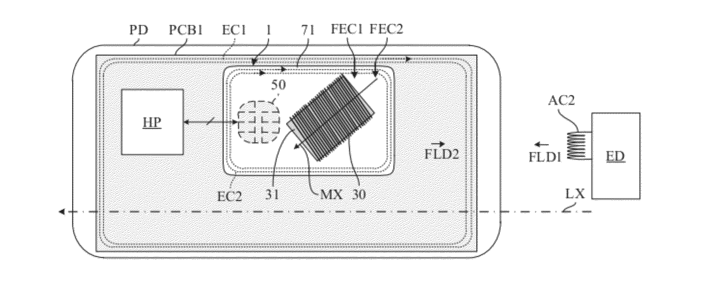
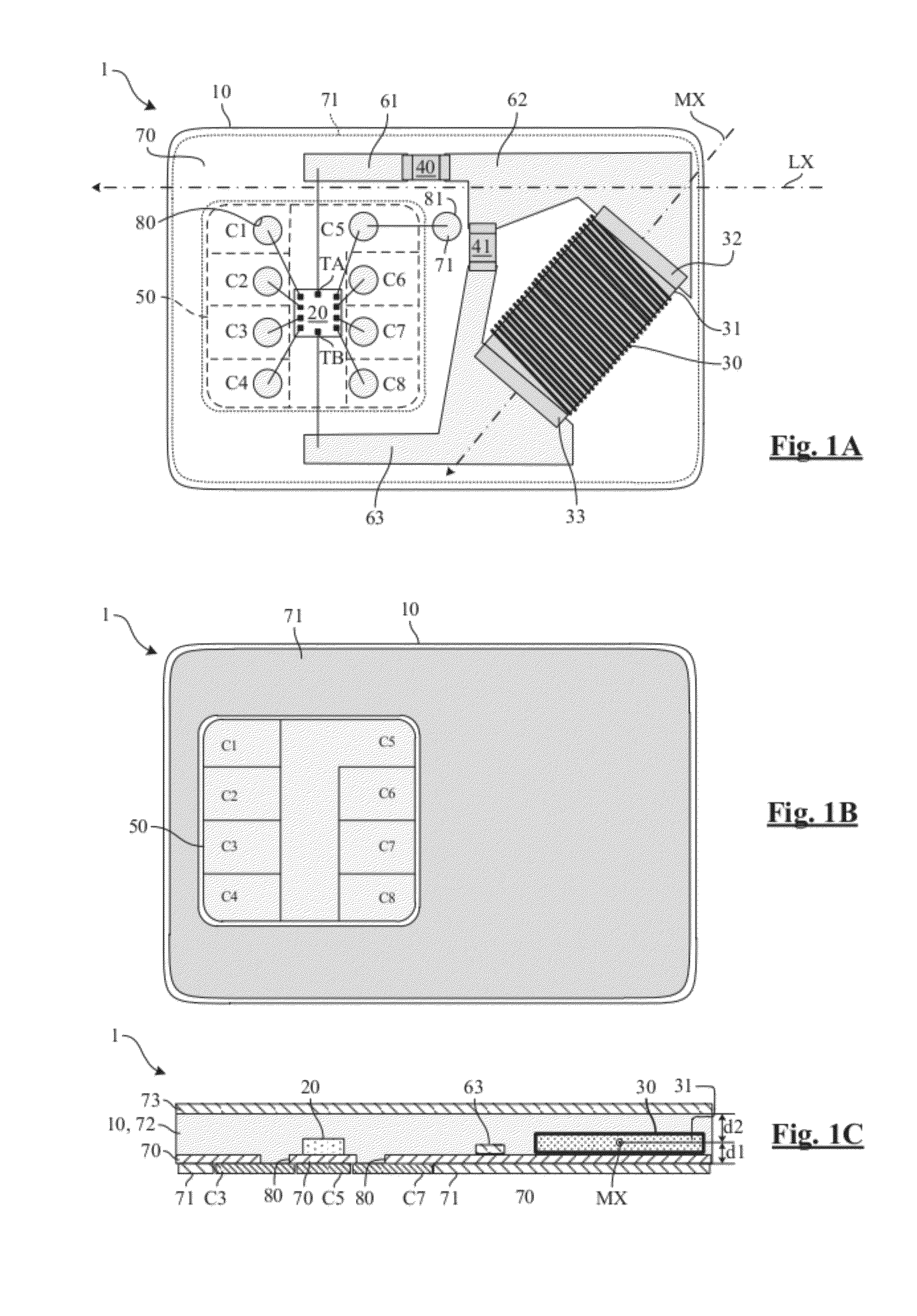
[0033]FIGS. 1A, 1B, 1C are respectively top, bottom, and cross-sectional views of an NFC card 1 according to the invention. The NFC card may be a SIM-NFC card intended to be inserted into a mobile phone. In FIG. 1A, internal elements of the card are shown through a material in which they are embedded.

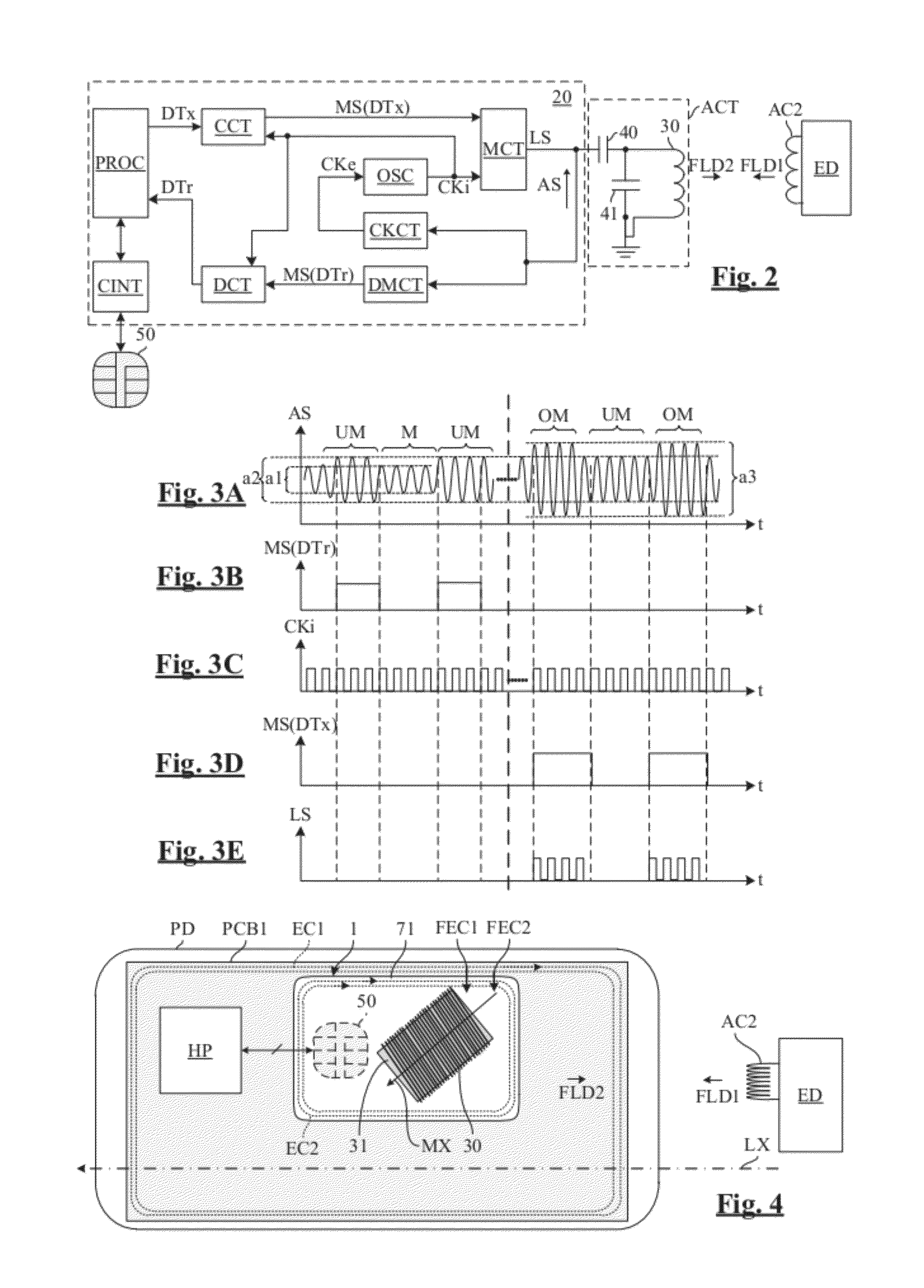
[0034]The NFC card 1 includes a plastic body 10, an integrated circuit 20, a tuned antenna circuit including an antenna coil 30 and tuning capacitors 40, 41, and a group 50 of contact pads (shown in dashed lines). The integrated circuit 20 is a dual contact / contactless device and is designed to perform both contact and contactless communications. The integrated circuit 20 may be a secure integrated circuit for a SIM-NFC card.

[0035]The group 50 of contact pads includes eight conventional ISO 7816 contacts C1 (Vcc), C2 (RST), C3 (CLK), C4 (RFU), C5 (GND), C6 (Vpp), C7 (I / O), and C8 (RFU) to which terminals of the integrated circuit 20 are linked. The integrated circuit 20 has additional t...


PUM


Abstract

An NFC card includes an antenna circuit including an antenna coil having at least one magnetic axis, and at least one integrated circuit linked to the antenna circuit. The magnetic axis of the antenna coil is substantially parallel to the plane of the card, and is at an angle of 45°±25° with respect to a longitudinal axis LX of the card. Embodiments of the invention are applicable in particular to SIM-NFC card and SD-NFC cards.

Description

BACKGROUND OF THE INVENTION[0001]Embodiments of the present invention relate to Near Field Communications cards (NFC cards), and more particularly to NFC cards intended to be inserted within a handheld device such as a mobile telephone. Embodiments of the present invention also relate to a method for performing a contactless communication between an NFC card and an external NFC device.[0002]Known NFC cards intended to be inserted within handheld devices are, for example, NFC Subscriber Identity Modules, also called SIM-NFC, or NFC Secure Digital (SD) cards. International Publication WO 98 / 58509 discloses a SIM-NFC card including contact pads, a microprocessor, an NFC module, and an antenna coil. The antenna coil has one or more coplanar coaxial windings parallel to the plane of the card, and therefore presents a magnetic axis perpendicular to the plane of the card. It can perform contact communications with the mobile telephone through the contact pads and an NFC communication with ...

Claims


Application Information

Patent Timeline
Patent Type & Authority Patents(United States)
IPC IPC(8): H04B5/00
CPCG06K19/07771G06K19/07769
Inventor CHARRAT, BRUNOCORDIER, NICOLAS
Owner VERIMATRIX INC
Learn More