Non-volatile memory element and manufacturing method thereof

a technology manufacturing methods, which is applied in the direction of bulk negative resistance effect devices, semiconductor devices, electrical devices, etc., can solve the problems of non-uniform characteristics of non-volatile memory elements, and achieve the reduction of non-uniform read currents corresponding to low-resistance states, easy to ensure a reading margin of current, and suppress non-uniform resistances

Active Publication Date: 2014-09-02
PANASONIC SEMICON SOLUTIONS CO LTD
View PDF13 Cites 2 Cited by
  • Summary
  • Abstract
  • Description
  • Claims
  • Application Information

AI Technical Summary

Benefits of technology

[0127]With the above described configuration, the redox reaction of the first metal oxide is enabled to selectively take place in a region in the vicinity of the interface of the first electrode, and the polarity with which resistance change occurs is always stabilized. In addition, the third metal oxide layer which is higher in relative content rate of oxygen serves to suppress non-uniformity of resistances in a region which is distant from the interface of the first electrode. Since non-uniformity of read currents corresponding to the low-resistance state can be lessened, while decreasing a switching current for changing the element to the low-resistance state, a difference between the read current corresponding to the low-resistance state and a read current corresponding to the high-resistance state increases (it becomes easier to ensure a margin of reading of the current). As a result, misdetermination as to whether the element is in the low-resistance state or in the high-resistance state is less likely to occur, and hence a read error is less likely to occur.Modified Example
[0128]The non-volatile memory 100 may include a substrate provided with a first wire, a first interlayer insulating layer comprising a silicon oxide layer (300 to 500 nm) formed on and above the substrate so as to cover the first wire, and a first contact plug (diameter: 50 to 300 nm Φ) formed so as to penetrate the first interlayer insulating layer such that the first contact plug is electrically connected to the first wire, and comprising tungsten as a major component.
[0129]Then, the second electrode 104 (in the present embodiment, lower electrode) may be formed on and above the first interlayer insulating layer so as to cover the first contact plug.
[0130]A second interlayer insulating layer comprising a silicon oxide layer (thickness: 300 to 500 nm) may be formed so as to cover the non-volatile memory element 100. A second contact plug (diameter: 50 to 300 nm Φ) comprising tungsten as a major component may be formed to penetrate the second interlayer insulating layer such that the second contact plug is electrically connected to the first electrode. The second wire may be formed on and above the second interlayer insulating layer so as to cover the second contact plug.
[0131]In the present embodiment, the first electrode 106 and the first metal oxide layer 115x are in contact with each other, while the second electrode 104 and the third metal oxide layer 115z are in contact with each other. In this case, the first electrode and the second electrode may comprise materials containing different elements as major components, and a standard electrode potential V1 of the first electrode, a standard electrode potential V2 of the second electrode, and a standard electrode potential Vt1 of the metal M constituting the first metal oxide layer may satisfy a relationship of Vt1<V1 and V2<V1.
[0132]In the present embodiment, for example, the first electrode 106 and the first metal oxide layer 115x are in contact with each other, the second electrode 104 and the third metal oxide layer 115z are in contact with each other, iridium (Ir) is used as the first electrode 106 and tantalum nitride (TaN) is used as the second electrode 104. The standard electrode potential V1 of iridium is 1.156V, while the standard electrode potential V2 of the tantalum nitride is 0.48V. In a case where the tantalum oxide is used as the variable resistance layer, Vt1<V1 and V2<V1 are satisfied because the standard electrode potential Vt of tantalum is −0.6V.

Problems solved by technology

The conventional non-volatile memory device has a problem that there is non-uniformity of characteristics of non-volatile memory elements.

Method used


Image

  • Non-volatile memory element and manufacturing method thereof
  • Non-volatile memory element and manufacturing method thereof
  • Non-volatile memory element and manufacturing method thereof

Examples


embodiment 1

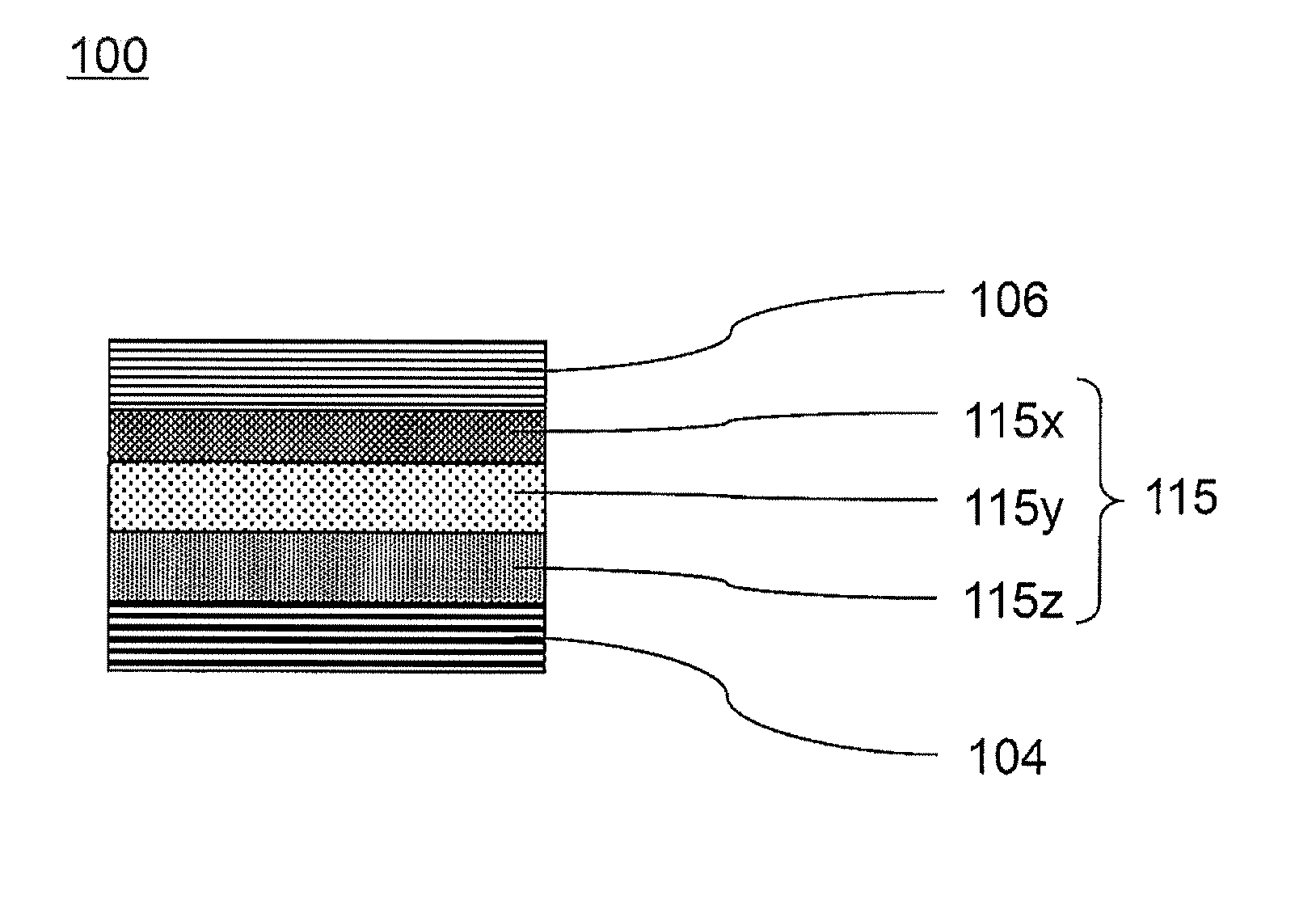
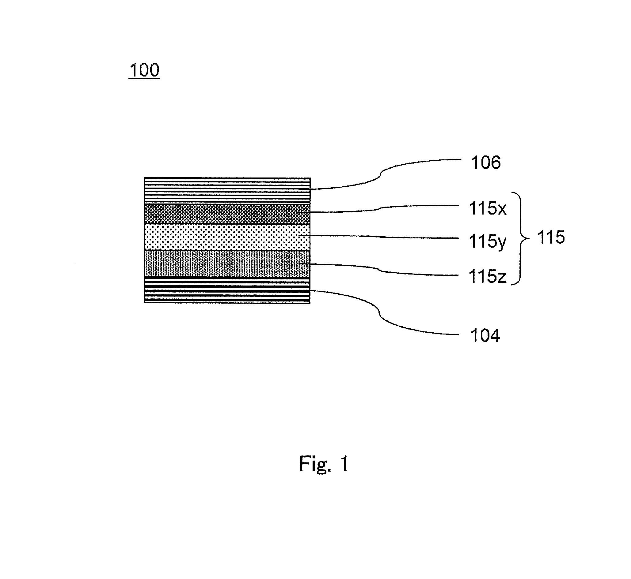
[0058]According to Embodiment 1, a non-volatile memory element comprises a first electrode; a second electrode; and a variable resistance layer which is interposed between the first electrode and the second electrode, and reversibly changes its resistance value in response to an electric signal applied between the first electrode and the second electrode; the variable resistance layer including, when a first metal is M and a second metal is N: a third metal oxide layer having a composition expressed as NOz; a second metal oxide layer having a composition expressed as NOy; and a first metal oxide layer having a composition expressed as MOx such that the third metal oxide layer, the second metal oxide layer and the first metal oxide layer are stacked in this order; wherein when an oxygen content atomic percentage of an oxide of the first metal M in a stoichiometric state is A, an oxygen content atomic percentage of an oxide of the second metal N in a stoichiometric state is B, an oxyg...

modified example

[0128]The non-volatile memory 100 may include a substrate provided with a first wire, a first interlayer insulating layer comprising a silicon oxide layer (300 to 500 nm) formed on and above the substrate so as to cover the first wire, and a first contact plug (diameter: 50 to 300 nm Φ) formed so as to penetrate the first interlayer insulating layer such that the first contact plug is electrically connected to the first wire, and comprising tungsten as a major component.

[0129]Then, the second electrode 104 (in the present embodiment, lower electrode) may be formed on and above the first interlayer insulating layer so as to cover the first contact plug.

[0130]A second interlayer insulating layer comprising a silicon oxide layer (thickness: 300 to 500 nm) may be formed so as to cover the non-volatile memory element 100. A second contact plug (diameter: 50 to 300 nm Φ) comprising tungsten as a major component may be formed to penetrate the second interlayer insulating layer such that th...

embodiment 2

[0175]A non-volatile memory element of Embodiment 2 is the nonvolatile memory element according to any of Embodiment 1 and modified examples of Embodiment 1, and is configured such that a second electrode is disposed above a first electrode.

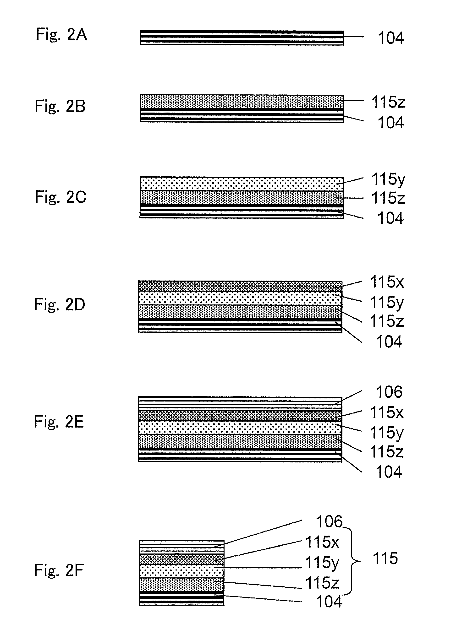
[0176]A manufacturing method of the non-volatile memory element of Embodiment 2 comprises the steps of forming the first electrode, forming a first metal oxide layer having a composition expressed as MOx (M: first metal) on and above the first electrode, depositing a second metal oxide layer having a composition expressed as NOy (N: second metal) on and above the first metal oxide layer, depositing a third metal oxide layer having a composition expressed as NOz on and above the third metal oxide layer, and forming the second electrode on and above the third metal oxide layer, wherein when an oxygen content atomic percentage of an oxide of the first metal M in a stoichiometric state is A, an oxygen content atomic percentage of an oxide of the seco...


PUM

PropertyMeasurementUnit
resistivityaaaaaaaaaa
thicknessaaaaaaaaaa

Abstract

A non-volatile memory element including a first electrode; a second electrode; and a variable resistance layer. The variable resistance layer including, when a first metal is M and a second metal is N: a third metal oxide layer NOz; a second metal oxide layer NOy; and a first metal oxide layer MOx such that the third, second and first metal oxide layers are stacked in this order; wherein when an oxygen content atomic percentage of an oxide of the first metal M in a stoichiometric state is A, an oxygen content atomic percentage of an oxide of the second metal N in a stoichiometric state is B, an oxygen content atomic percentage of MOx is C, an oxygen content atomic percentage of NOy is D, and an oxygen content atomic percentage of NOz is E, (D / B)<(C / A), (E / B)<(C / A) and y<z are satisfied.

Description

CROSS-REFERENCE TO RELATED PATENT APPLICATION[0001]The application claims priority to Japanese Patent Application No. 2012-211751, filed on Sep. 26, 2012, the entire disclosure of which is incorporated herein by reference.BACKGROUND OF THE INVENTION[0002]1. Field of the Invention[0003]The present invention relates to a non-volatile memory element and a manufacturing method thereof. More particularly, the present invention relates to a variable resistance non-volatile memory element which changes its resistance value in response to an electric signal applied thereto.[0004]2. Description of the Related Art[0005]In recent years, with progresses of digital technologies, electronic devices such as portable information devices and information home electric appliances have been developed to provide higher functionalities. With achievement of the higher functionalities of these electronic devices, further miniaturization and higher-speeds of semiconductor elements incorporated into these el...

Claims


Application Information

Patent Timeline
Patent Type & Authority Patents(United States)
IPC IPC(8): H01L47/00H01L45/00
CPCH01L45/146H01L45/1608H01L45/08H01L45/1233H01L45/1625H01L45/1675H10N70/24H10N70/026H10N70/8833H10N70/826H10N70/063H10N70/021
Inventor YASUHARA, RYUTARONINOMIYA, TAKEKITAKAGI, TAKESHI
Owner PANASONIC SEMICON SOLUTIONS CO LTD
Why Eureka
Try Eureka