
Light Emitting Element and Illumination Device

a technology illumination devices, which is applied in the direction of semiconductor devices, basic electric elements, electrical equipment, etc., can solve the problems of high emission intensity, insufficient diffusion of electrical current from an electrode pad disposed on the p-type semiconductor layer, and low luminous efficiency of light emitting elements using semiconductors. achieve the effect of suppressing the non-uniformity of emission intensity distribution and improving light extraction efficiency

Inactive Publication Date: 2010-11-18
KYOCERA CORP
View PDF8 Cites 3 Cited by
  • Summary
  • Abstract
  • Description
  • Claims
  • Application Information

AI Technical Summary

Benefits of technology

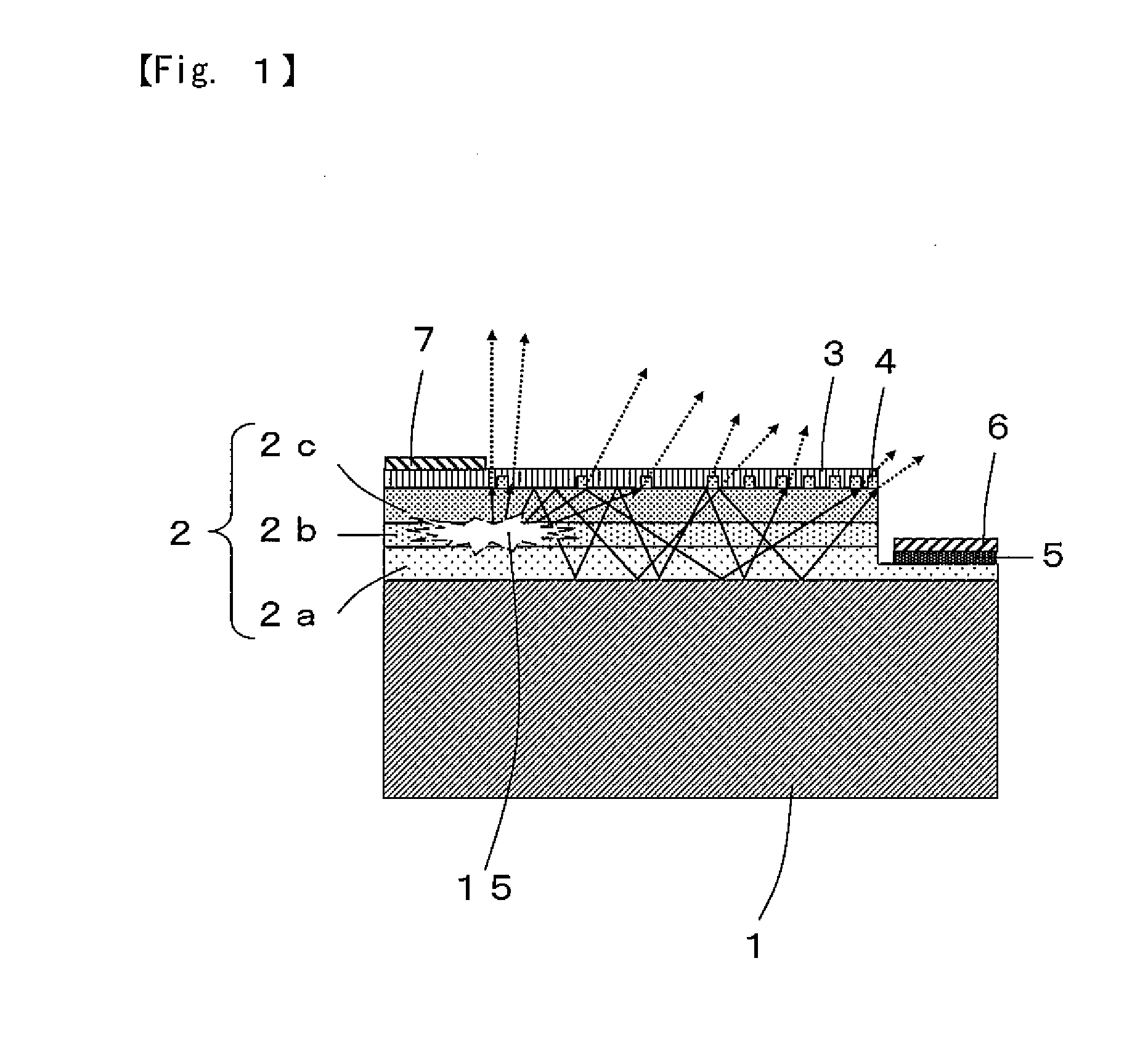
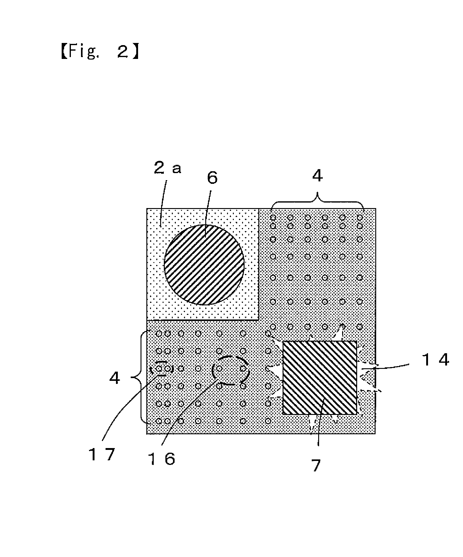
The present invention provides a light emitting element that improves the efficiency of light extraction and reduces the unevenness of emission intensity distribution over the entire surface of a light extraction surface. The light emitting element includes a semiconductor multilayer body with projections on one main surface through which light is emitted. The main surface has two regions separated by an interval between the projections, with the projections in the second region being closer to the electrode pad than those in the first region.

Problems solved by technology

However, the luminous efficiency of the light emitting elements using the semiconductor is lower than that of the fluorescent lamps, and hence they are required to achieve higher efficiency.
Therefore, the electrical current injected from an electrode pad disposed on the p-type semiconductor layer cannot be sufficiently diffused into the p-type semiconductor layer, and shows high emission intensity in the vicinity of the electrode pad.
Consequently, a uniform emission intensity distribution cannot be obtained over the entire surface of the light emitting element.

Method used


Image

  • Light Emitting Element and Illumination Device
  • Light Emitting Element and Illumination Device
  • Light Emitting Element and Illumination Device

Examples


example 2

[0071]A simulation was carried out using the light emitting element shown in FIG. 4. The shape of an n-type gallium nitride compound semiconductor layer 2a when viewed from above was a square (340 μm×340 μm). A transparent conductive layer 3 composed of ITO was deposited so as to cover the upper surface of a p-type gallium nitride compound semiconductor layer 2c. Thereafter, a p-electrode pad 7 connected to the p-type gallium nitride compound semiconductor layer 2c was formed at a corner part of the upper surface of the transparent conductive layer 3. The p-electrode pad 7 was a square of 100 μm×100 μm and composed of gold (Au). A part of a substrate 1 was inclined so that the main surface of a semiconductor multilayer body 2 on the inclined surface of the substrate 1 was inclined 30 degrees with respective to a noninclined surface.

[0072]A large number of projections 4 were formed on the upper surface of the p-type gallium nitride compound semiconductor layer 2c. When the distance o...


PUM


Abstract

Provided is a light emitting element capable of improving light extraction efficiency and suppressing the nonuniformity of emission intensity distribution over the entire surface of a light extraction surface. The light emitting element is provided with a semiconductor multilayer body having an n-type semiconductor layer and an emission layer and a p-type semiconductor layer, and an electrode pad connected to the p-type semiconductor layer. The semiconductor multilayer body has a large number of projections on one main surface thereof through which the light from the emission layer is emitted. The main surface of the semiconductor multilayer body has a first region located in the vicinity of the electrode pad, and a second region being further separated from the electrode pad than the first region. The interval between the projections in the second region is smaller than that in the first region.

Description

TECHNICAL FIELD[0001]The present invention relates to a light emitting element, such as a light emitting diode (LED), and an illumination device.BACKGROUND ART[0002]Recently, light emitting elements using a semiconductor such as a nitride-based semiconductor have been attracting attention.[0003]Owing to low energy consumption and long luminous life of the light emitting elements using the semiconductor, these light emitting elements have been put into practice as a replacement for incandescent light bulbs or fluorescent lamps. However, the luminous efficiency of the light emitting elements using the semiconductor is lower than that of the fluorescent lamps, and hence they are required to achieve higher efficiency.[0004]As a method of improving light extraction efficiency that is a technique for increasing the efficiency of the light emitting elements, there is, for example, a method of forming an concave and convex structure on the surface of a light emitting element (for example, r...

Claims


Application Information

Patent Timeline
Patent Type & Authority Applications(United States)
IPC IPC(8): H01L33/02H01L33/30H01L33/44H01L33/20H01L33/22
CPCH01L33/22H01L33/20
Inventor KAWAGUCHI, YOSHIYUKINISHIZONO, KAZUHIRO
Owner KYOCERA CORP
Learn More