Nano-imprint mold

a technology of nano-imprinting and molds, which is applied in the direction of dough shaping, manufacturing tools, electric/magnetic/electromagnetic heating, etc., can solve the problems of variation or degradation of the properties of the thickness of residual resin layers with the pattern of projections and recesses transferred thereto, so as to reduce the manufacturing cost of devices such as distributed feedback laser diodes

Active Publication Date: 2014-09-09
SUMITOMO ELECTRIC IND LTD
View PDF10 Cites 2 Cited by
  • Summary
  • Abstract
  • Description
  • Claims
  • Application Information

AI Technical Summary

Benefits of technology

[0006]Semiconductor optical devices have fine patterns. In order to manufacture such semiconductor optical devices, the use of a nano-imprint technique is under consideration. An example of a fine pattern in a semiconductor optical device includes a diffraction grating. A diffraction grating is, for example, included in a distributed feedback laser diode. A diffraction grating has periodic projections and recesses with a period of about 200 nm and a depth of about 50 to 300 nm. Using a nano-imprint technique to form such a fine pattern is advantageous in that the manufacturing cost of the device, such as a distributed feedback laser diode, can be reduced.
[0012]To reduce the variation in the shape of the fine patterns caused by the surface roughness of the semiconductor substrate described above, a step of pressing the mold firmly against the semiconductor substrate can be contained for forming the fine patterns. However, a semiconductor substrate, especially, a group III-V compound semiconductor substrate, generally breaks easily when the mold is firmly pressed against the substrate. In addition, a crystal defect, such as a dislocation, is probably introduced in the semiconductor substrate by pressing the mold firmly against the semiconductor substrate. Therefore, it is not preferable to include a step of pressing the mold firmly against the semiconductor substrate in forming the fine patterns.
[0014]In the nano-imprint mold according to the present invention, the bulk modulus of the elastic body disposed between the mold base and the mold body is lower than the bulk modulus of the mold body. Therefore, when the second surface of the mold is pressed against a resin portion formed on a substrate in a nano-imprint process, the elastic body deforms so that the second surface of the mold becomes substantially parallel to the surface of the substrate. In other words, when the mold is pressed against the resin portion, the elastic body deforms so that the distance between the second surface of the mold and the surface of the substrate becomes substantially constant. Accordingly, even when the surface of the substrate is uneven in height, a fine pattern formed on the second surface of the mold body is exactly transferred to the resin portion without deformation or changing in the shape of the pattern.
[0017]According to the nano-imprint mold in the embodiment, the protrusion protects the second surface of the mold body against damage in pressing the pattern surface on the resin portion. Furthermore, when the mold is pressed against the resin portion, the protrusion does not contact the surface of the resin portion. Therefore, the protrusion does not affect the resin patterns in the resin portion in pressing the pattern surface on the resin portion.
[0021]When the thickness of the mold body from the first surface to the second surface is 0.5 mm or smaller, the mold body can sufficiently bend when the mold is pressed against the resin portion. Therefore, the second surface of the mold becomes even more substantially parallel to the surface of the substrate. Accordingly, even when the surface of the substrate is uneven in height, a fine pattern formed on the second surface of the mold body is exactly transferred to the resin portion without deformation or changing in the shape of the pattern.
[0022]If the thickness of the mold body from the first surface to the second surface is 0.1 mm or greater, deformation of the pattern in the second surface can be sufficiently reduced in pressing the mold against the resin portion. As a result, the fine pattern of the mold body is exactly transferred to the resin portion without deformation or changing in the shape of the pattern due to the bending of the mold body.

Problems solved by technology

If the surface of the semiconductor layer and the pattern surface of the mold have poor parallelism therebetween, the thickness of the residual resin layer with the pattern of projections and recesses transferred thereto would not be uniform.
However, if the surface of the semiconductor layer and the pattern surface of the mold have poor parallelism therebetween, the thickness of the residual resin layer would not be uniform.
If the distributed feedback laser diode has a diffraction grating with a variation in the shape and height (or depth) of the projections and recesses, this variation in the shape and height (or depth) can lead to a variation or degradation in the properties of the distributed feedback laser diode.

Method used


Image

  • Nano-imprint mold
  • Nano-imprint mold
  • Nano-imprint mold

Examples


first embodiment

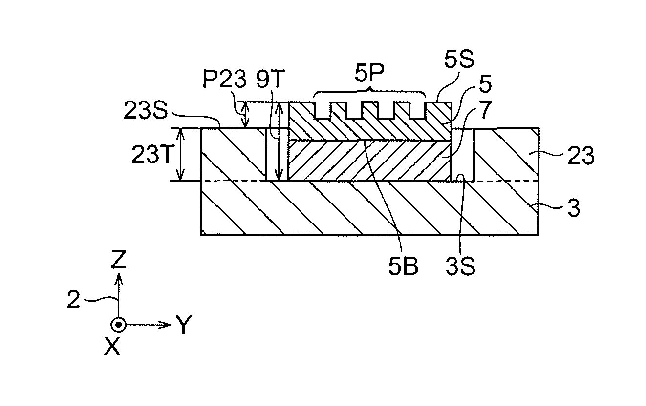
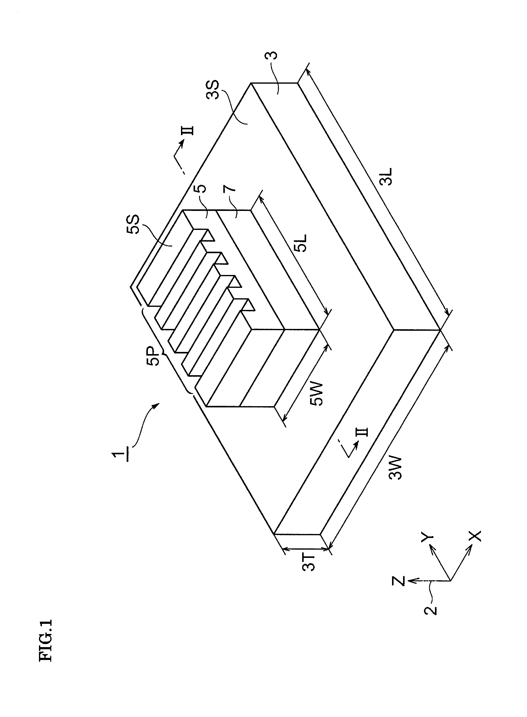
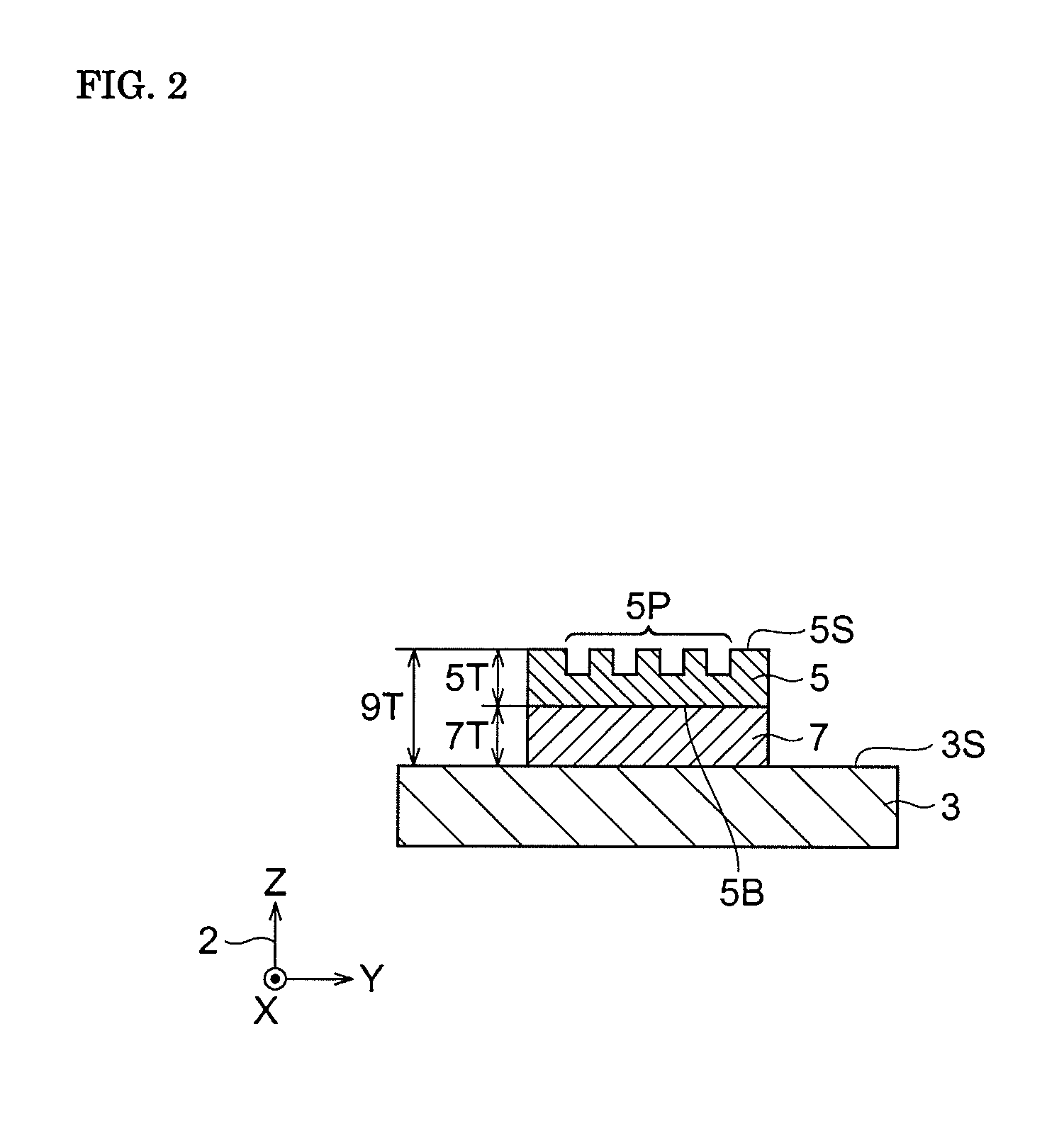
[0039]FIG. 1 is a perspective view of a nano-imprint mold according to a first embodiment. FIG. 2 is a cross-sectional view of the nano-imprint mold taken along line II-II in FIG. 1.

[0040]As shown in FIGS. 1 and 2, a nano-imprint mold 1 according to this embodiment includes a mold base 3, a mold body 5, and an elastic body 7 disposed between the mold base 3 and the mold body 5. In FIGS. 1 and 2, an orthogonal coordinate system 2 is shown.

[0041]In this embodiment, the mold base 3 is a rectangular plate with its thickness direction extending along a Z axis, and has a surface 3S extending along an X-Y plane. The mold base 3 is composed of, for example, quartz, synthetic quartz, silicon, nickel, or the like. If ultraviolet curing resin is to be used as a nano-imprint resin portion to be described later, the mold base 3 is preferably composed of a material with sufficient ultraviolet transmissivity, such as quartz or synthetic quartz.

[0042]For example, the mold base 3 has, for example, t...

second embodiment

[0073]Next, a nano-imprint mold according to a second embodiment will be described. FIG. 12 is a perspective view of the nano-imprint mold according to this embodiment. FIG. 13 is a cross-sectional view of the nano-imprint mold taken along line XIII-XIII in FIG. 12.

[0074]A nano-imprint mold 1x according to this embodiment shown in FIGS. 12 and 13 differs from the mold 1 according to the first embodiment in additionally having a protrusion 23.

[0075]The mold 1x according to this embodiment includes the protrusion 23 provided on the surface 3S of the mold base 3. As viewed in the thickness direction of the mold base 3, the protrusion 23 in this embodiment is separated from the mold body 5 and the elastic body 7. Moreover, the protrusion 23 is provided continuously along the outer edges of the mold base 3. The mold body 5 and the elastic body 7 are surrounded by the protrusion 23. The protrusion 23 is fixed to the mold base 3.

[0076]In this embodiment, the protrusion 23 is composed of th...


PUM

PropertyMeasurementUnit
thicknessaaaaaaaaaa
bulk modulusaaaaaaaaaa
depthaaaaaaaaaa

Abstract

A nano-imprint mold includes a mold base; mold body having a first surface and a second surface opposite the first surface; and an elastic body disposed between a surface of the mold base and the first surface of the mold body, the elastic body being composed of resin. The second surface of the mold body is provided with a nano-imprint pattern. In addition, the elastic body has a bulk modulus lower than a bulk modulus of the mold body.

Description

BACKGROUND OF THE INVENTION[0001]1. Field of the Invention[0002]The present invention relates to nano-imprint molds.[0003]2. Description of the Related Art[0004]Japanese Unexamined Patent Application Publication No. 2000-323461 discusses a fine-pattern forming method by a nano-imprint technique. According to this method, a mold used for nano-imprinting is made of an optically transparent material so that a wafer and the mold can be aligned with each other.[0005]“Fabrication of Nanometer Sized Features on Non-Flat Substrates Using a Nano-Imprint Lithography Process”, M. Miller, et. al., Proc. SPIE 5751, 994, pp. 995-998 (2005) discusses a fine-processing method using a nano-imprint technique. In this fine-processing method, a step-and-repeat technique is used. The fine-processing method involves preparing a mold having a master transfer pattern, forming a resin portion composed of ultraviolet curing resin on a substrate to be fine-processed, pressing the mold against a predetermined ...

Claims


Application Information

Patent Timeline
Patent Type & Authority Patents(United States)
IPC IPC(8): B29C59/02B29C43/02B29C43/06B29C43/14B82Y20/00
CPCB82Y20/00B29C43/021B29C43/06B29C2043/142
Inventor TSUJI, YUKIHIROYANAGISAWA, MASAKI
Owner SUMITOMO ELECTRIC IND LTD
Why Eureka
Try Eureka