Metal-on-metal (MoM) capacitors having laterally displaced layers, and related systems and methods

a technology of metal-on-metal and capacitors, applied in the field of capacitors, can solve the problems of increasing local stress, layered approach (whether with rotation), and capacitor footprint, and achieves the effect of reliably uniform capacitors, reducing cumulative surface process variations, and reducing the variance between two capacitors

Inactive Publication Date: 2014-09-16
QUALCOMM INC
View PDF11 Cites 8 Cited by
  • Summary
  • Abstract
  • Description
  • Claims
  • Application Information

AI Technical Summary

Benefits of technology

[0009]Embodiments disclosed in the detailed description include metal-on-metal (MoM) capacitors having laterally displaced layers. Related systems and methods are also disclosed. MoM capacitors according to the embodiments disclosed herein include a plurality of vertically stacked layers that are laterally displaced relative to one another. In an exemplary embodiment, the orientation of the lateral displacement alternates. As used herein, lateral displacement means displacement in a direction substantially perpendicular to a primary axis of the conductive element. Staggered or alternating lateral displacement of the layers minimizes cumulative surface process variations as the MoM capacitor layers are disposed on top of each other in a semiconductor to form the MoM capacitor. As a result, the variances between two capacitors made according to this process are relatively small, in effect, making more reliably uniform capacitors by effectively increasing the lithography and etching process windows. Since the process makes more uniform capacitors, circuit designers can more reliably use such capacitors in their designs.

Problems solved by technology

However, such larger nodes increase the footprint of the capacitor, defeating the miniaturization goals, and such larger nodes conflict with the process window and increase local stress significantly.
However, this layered approach (whether with rotation or not) suffers from cumulative errors resulting from misalignments of the conductive elements during the manufacturing process.
At a minimum, each inter-metal dielectric (IMD) surface will cause the next film surface to have the same irregularity and such irregularity will negatively affect the process window.
Further, it is possible that each additional layer will exaggerate the irregularity.

Method used


Image

  • Metal-on-metal (MoM) capacitors having laterally displaced layers, and related systems and methods
  • Metal-on-metal (MoM) capacitors having laterally displaced layers, and related systems and methods
  • Metal-on-metal (MoM) capacitors having laterally displaced layers, and related systems and methods

Examples


Embodiment Construction

[0026]With reference now to the drawing figures, several exemplary embodiments of the present disclosure are described. The word “exemplary” is used herein to mean “serving as an example, instance, or illustration.” Any embodiment described herein as “exemplary” is not necessarily to be construed as preferred or advantageous over other embodiments.

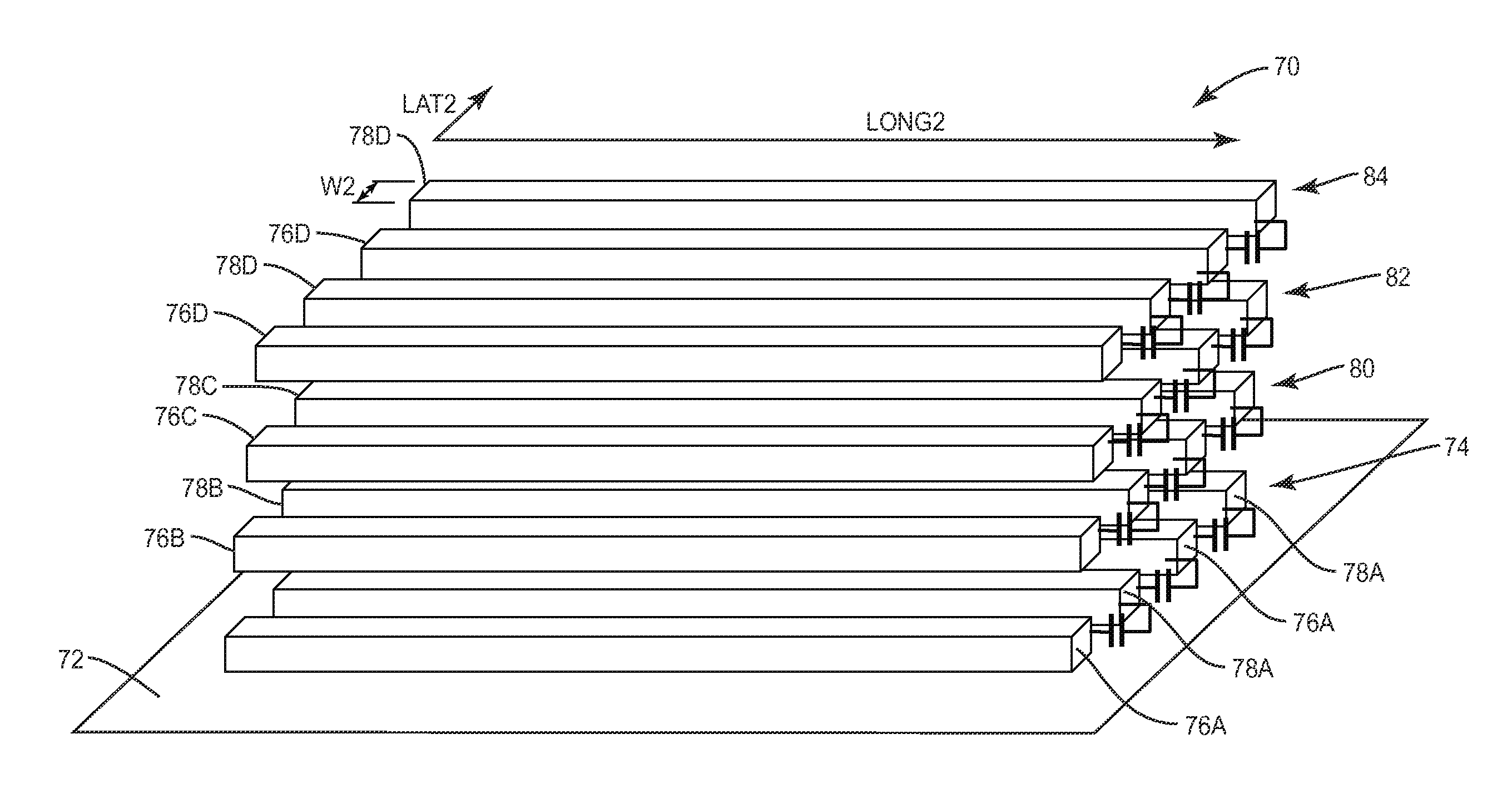
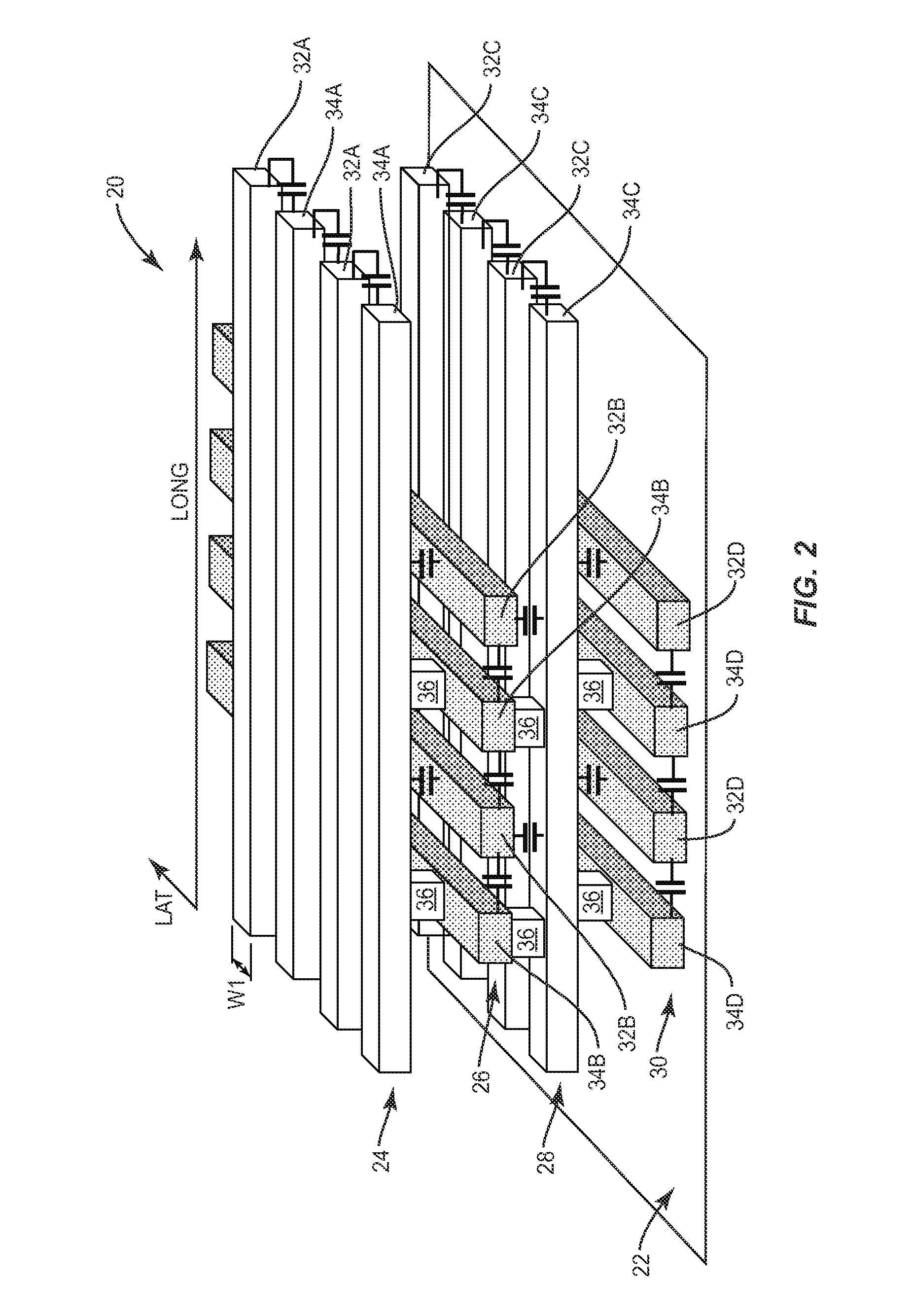
[0027]Embodiments disclosed in the detailed description include metal-on-metal (MoM) capacitors having laterally displaced layers. Related systems and methods are also disclosed. MoM capacitors according to the embodiments disclosed herein include a plurality of vertically stacked layers that are laterally displaced relative to one another. In an exemplary embodiment, the orientation of the lateral displacement alternates. As used herein, lateral displacement means displacement in a direction substantially perpendicular to a primary axis of the conductive element. Staggered or alternating lateral displacement of the layers minimizes cumula...


PUM


Abstract

Metal-on-Metal (MoM) capacitors having laterally displaced layers and related systems and methods are disclosed. In one embodiment, a MoM capacitor includes a plurality of vertically stacked layers that are laterally displaced relative to one another. Lateral displacement of the layers minimizes cumulative surface process variations making a more reliable and uniform capacitor.

Description

BACKGROUND[0001]I. Field of the Disclosure[0002]The technology of the disclosure relates to providing capacitors in semiconductor dies for use by integrated circuits.[0003]II. Background[0004]Mobile communication devices have become common in current society. The prevalence of these mobile devices is driven in part by the many functions that are now enabled on such devices. Demand for such functions increases processing capability requirements and generates a need for more powerful batteries. Within the limited space of the housing of the mobile communication device, batteries compete with the processing circuitry. These and other factors contribute to a continued miniaturization of components within the circuitry.[0005]Miniaturization of the components impacts all aspects of the processing circuitry including the transistors and other reactive elements in the processing circuitry, such as capacitors. One miniaturization technique involves moving some reactive elements from the prin...

Claims


Application Information

Patent Timeline
Patent Type & Authority Patents(United States)
IPC IPC(8): H01L21/02
CPCH01L28/60H01L23/5223H01L28/91H01L28/88H01L2924/0002H01L2924/00
Inventor LI, XIAYANG, BIN
Owner QUALCOMM INC
Why Eureka
Try Eureka