Supercharge Your Innovation With Domain-Expert AI Agents!

Pixel matrix with compensation of ohmic drops on the power supplies

a power supply and ohmic drop technology, applied in the field of microelectronic devices, can solve problems such as greater current consumption at the sour

Inactive Publication Date: 2014-10-14
COMMISSARIAT A LENERGIE ATOMIQUE ET AUX ENERGIES ALTERNATIVES
View PDF8 Cites 1 Cited by
  • Summary
  • Abstract
  • Description
  • Claims
  • Application Information

AI Technical Summary

Benefits of technology

[0025]The consumption of the current source transistors especially depends on a difference between the gate potential and the source potential of these transistors. This invention thus provides for the use of means to compensate an ohmic drop in one or several lines carrying the source potential of the current transistors by creating a corresponding decrease of the gate potentials, in order to obtain a difference in potentials between gate and source, that is constant from one current source transistor to another. The generating means are provided so that the change or variation of potentials along said first connection line, is able to compensate the decrease in source potentials in one or several source biasing line(s).
[0034]According to one possible embodiment, the current gain of the current mirrors may be equal to 1 / K (where K>1), wherein the additional conductor line has a linear resistance equal to or around 1 / K the linear resistance of the source biasing lines. This permits the impedance to be reduced below which the gate potentials are supplied.

Problems solved by technology

In return, the application of the potential Vs to the source of the transistor T1 causes greater consumption of current at the source.

Method used


Image

  • Pixel matrix with compensation of ohmic drops on the power supplies
  • Pixel matrix with compensation of ohmic drops on the power supplies
  • Pixel matrix with compensation of ohmic drops on the power supplies

Examples


Embodiment Construction

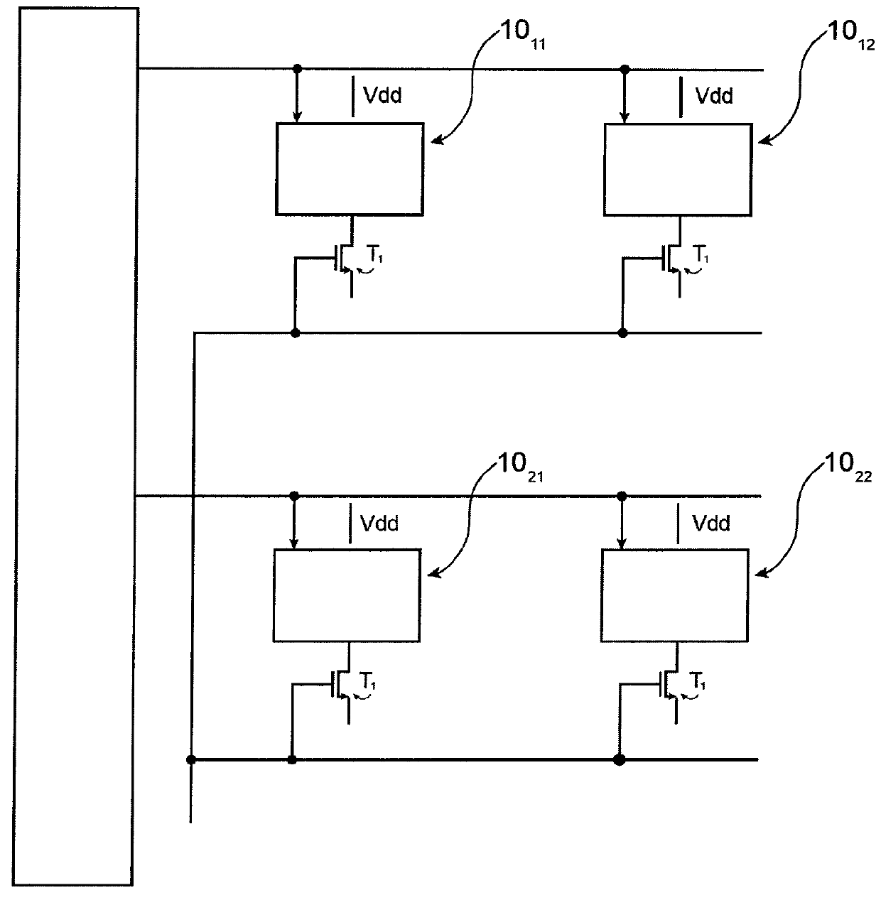
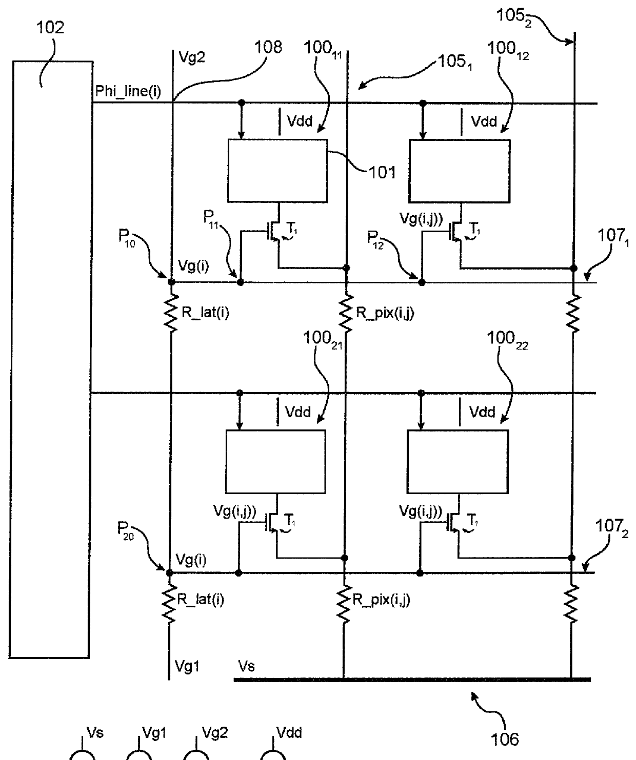
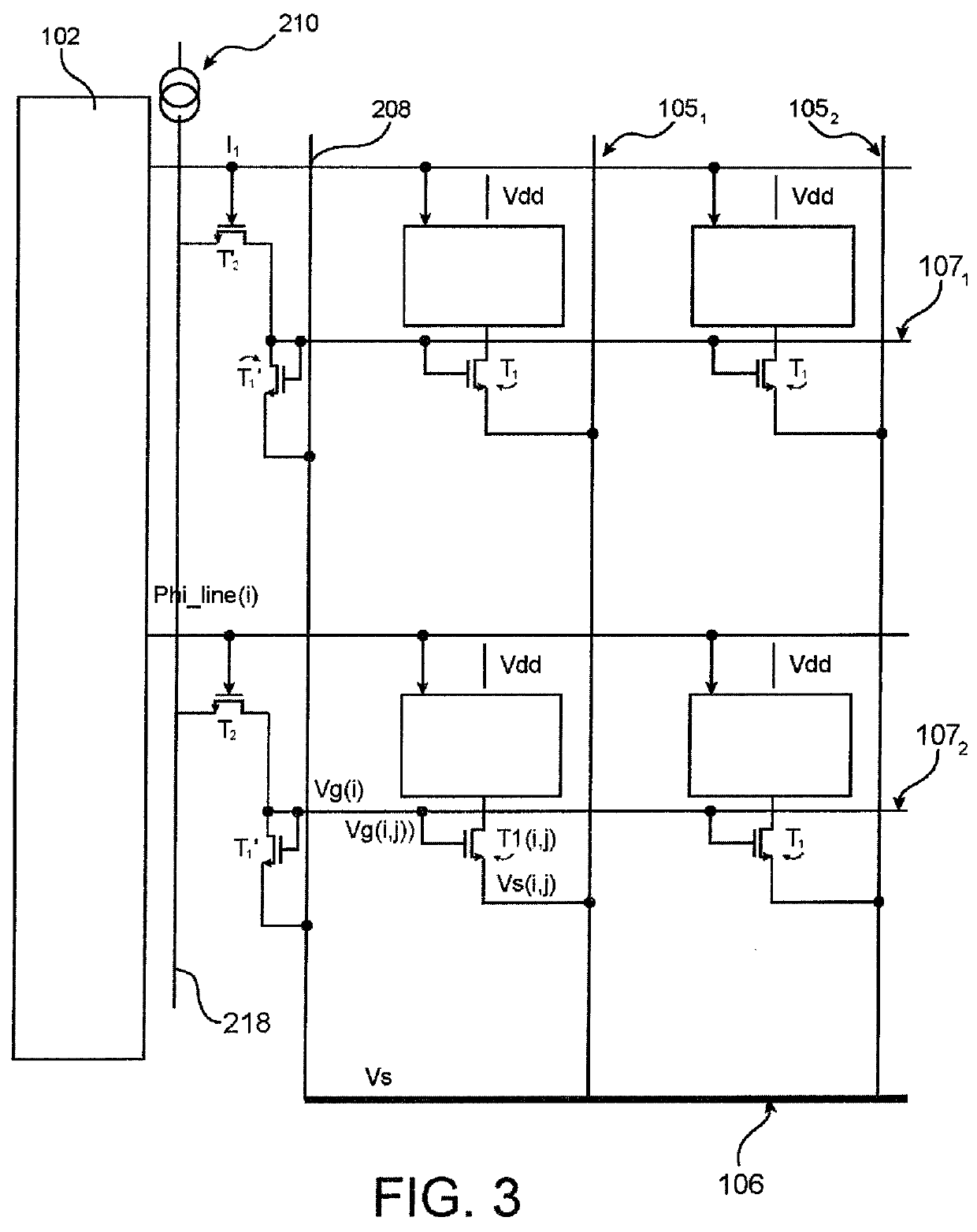
[0016]The invention relates to a matrix microelectronic device comprising:[0017]a plurality of elementary cells laid out according to a matrix, respectively comprising at least one current source formed by at least one current source transistor,[0018]a source electrode of said transistor is connected to a source biasing conductor line among a plurality of source biasing conductor lines,[0019]a gate electrode of said transistor is connected to a gate biasing conductor line among a plurality of conductor gate biasing lines,

[0020]wherein the device is further equipped with means for biasing conductor gate biasing lines comprising:[0021]at least one first connection line that may be connected to one or several of said conductor gate biasing lines,[0022]means for generating, current or voltage, positioned on at least one end of said first connection line, and designed to generate a change or evolution or variation, for example a decrease, in the potentials along said first connection lin...


PUM


Abstract

A matrix microelectronic device includes elementary cells laid out according to a matrix. Each cell has a current source formed by a current source transistor. A source electrode of the transistor is connected to a source biasing conductor line of a plurality of source biasing conductor lines. A gate electrode of the transistor is connected to a gate biasing conductor line of a plurality of gate biasing conductor lines. A biasing device biases the gate biasing conductor lines and includes at least one first connection line that is connected to at least several of the gate biasing conductor lines. The biasing device includes a voltage generator or a current generator that causes a variation of potentials along the first connection line, thereby compensating a corresponding variation of potentials along the source biasing conductor lines. The device can include an addressing circuit for addressing horizontal lines or rows of the matrix.

Description

TECHNICAL FIELD[0001]The invention relates to the field of microelectronic devices formed by elementary cells or matrix pixels and especially applies to large matrices that have a current source in each pixel, for example X-ray detector matrices.[0002]The invention permits homogeneous consumption and performances to be obtained between the pixels or elementary cells of a matrix device in which the cells are respectively equipped with a current source.[0003]The invention provides for the use of a matrix microelectronic device formed by elementary cells respectively comprising a current source whose consumption depends on a difference of two biasing potentials, and means for compensating an ohmic drop in one or several lines carrying one of said two potentials to the pixels.STATE OF THE PRIOR ART[0004]In a matrix microelectronic device, such as an X-ray detector matrix, the signals sent from the elementary cells or pixels of the matrix are generally read by scanning the horizontal lin...

Claims


Application Information

Patent Timeline
Patent Type & Authority Patents(United States)
IPC IPC(8): G01T1/24H01L25/00H01L27/00H04N5/32H04N5/369H04N5/374
CPCH04N5/32H04N5/3698H04N5/374H04N25/677H04N25/709H04N25/76H04N25/77
Inventor PEIZERAT, ARNAUDARQUES, MARCMARTIN, JEAN-LUC
Owner COMMISSARIAT A LENERGIE ATOMIQUE ET AUX ENERGIES ALTERNATIVES
Features
  • R&D
  • Intellectual Property
  • Life Sciences
  • Materials
  • Tech Scout
  • Unparalleled Data Quality
  • Higher Quality Content
  • 60% Fewer Hallucinations
Learn More