Laminated body, circuit board including laminated body, semiconductor package and process for manufacturing laminated body

a technology of laminated body and circuit board, which is applied in the direction of packaging, textiles and paper, and synthetic resin layered products, etc., can solve the problems of increasing the warpage of the core itself, the warpage of the conventional core substrate, and the warpage of the laminated body. the effect of minimizing the warpage and minimizing the warpag

Inactive Publication Date: 2014-10-28
SUMITOMO BAKELITE CO LTD
View PDF14 Cites 3 Cited by
  • Summary
  • Abstract
  • Description
  • Claims
  • Application Information

AI Technical Summary

Benefits of technology

[0007]A resin-impregnated laminated body with fibers such as a glass cloth as a base material has excellent rigidity and is suitable for the use as a thin core base material. However, as a core substrate has been thinner, the problem of a warpage in a conventional core substrate has become more significant. A thinner core substrate tends to result in a larger warpage, which leads to the problems of increase in a warpage of a core itself and increase in a warpage of a package caused by the increase in a warpage of a core.
[0009]In view of the situation described above, the present invention provides a laminated body with a reduced warpage by controlling misalignment between overlapped fibers in a fibrous base material, a circuit board having a laminated body, a semiconductor package and a process for manufacturing a laminated body.
[0010]The present invention is based on the observation that a warpage in a laminated body can be reduced by reducing a misalignment between fibers due to bowing, paying attention to the presence of a bowing in a fibrous base material.
[0053]In the above manufacturing processes of the present invention, fibrous base materials are laminated such that misalignment of fibers between the fibrous base materials is reduced, to minimize a warpage in a laminated body as a final product.
[0054]Briefly, the present invention provides a process for manufacturing a laminated body where a warpage is minimized. In the process of the present invention, when laminating two or more fibrous base materials, misalignment of fibers can be controlled to minimize a warpage in a laminated body itself as a final product. Furthermore, the present invention provides a laminated body where a warpage is minimized. A laminated body according to the present invention is suitable for a thin core material in a semiconductor package.

Problems solved by technology

However, as a core substrate has been thinner, the problem of a warpage in a conventional core substrate has become more significant.
A thinner core substrate tends to result in a larger warpage, which leads to the problems of increase in a warpage of a core itself and increase in a warpage of a package caused by the increase in a warpage of a core.
However, attention has been little focused on the presence of such a bowing region.
We have found that when two or more fibrous base materials are laminated, the presence of the bowing region causes misalignment between overlapped fibers, which finally influences warpage in a core material.
The above patent applications do not pay attention to the presence of a bowing region in a fibrous base material and thus has not yet solve the problem of warpage caused by thinning a core material.

Method used


Image

  • Laminated body, circuit board including laminated body, semiconductor package and process for manufacturing laminated body
  • Laminated body, circuit board including laminated body, semiconductor package and process for manufacturing laminated body
  • Laminated body, circuit board including laminated body, semiconductor package and process for manufacturing laminated body

Examples


example 1

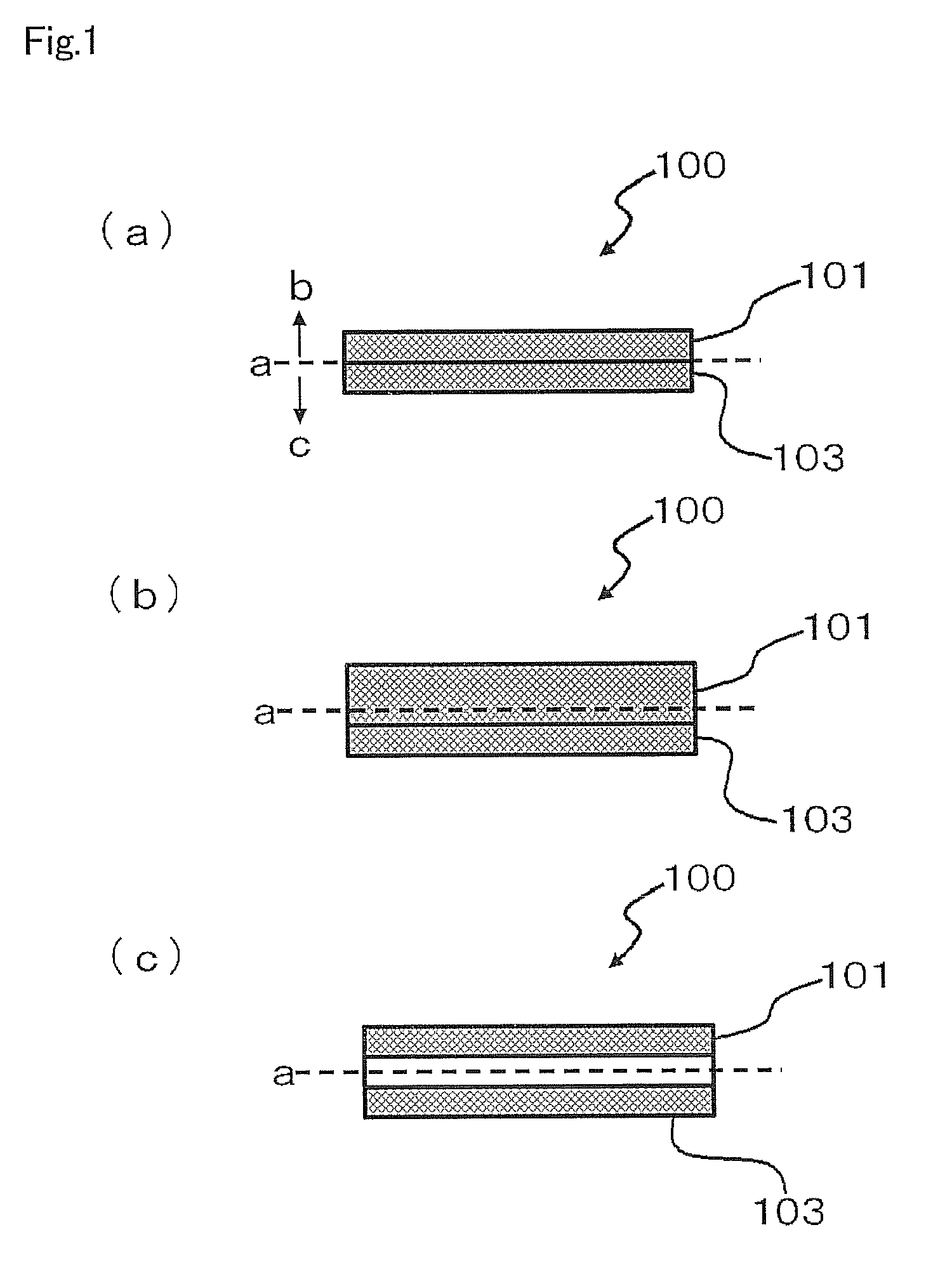
[0186]A laminated body with a copper foil was manufactured as described below.

(1) Preparation of a Resin Varnish

[0187]19.7 parts by weight of a novolac type cyanate resin (Lonza Japan Ltd., Primaset PT-30, weight-average molecular weight: about 700), 11 parts by weight of a biphenyldimethylene type epoxy resin (Nippon Kayaku Co., Ltd., NC-3000H, epoxy equivalent: 275), 9 parts by weight of a biphenyldimethylene type phenol resin (Meiwa Plastic Industries, Ltd., MEH-7851-3H, hydroxide equivalent: 230) and 0.3 parts by weight of an epoxy silane type coupling agent (GE Toshiba Silicones Co., Ltd., A-187) were dissolved in methyl ethyl ketone at an ambient temperature, and 60 parts by weight of a spherical fused silica (Admatechs Co. Ltd., spherical fused silica, SO-25R, average particle size: 0.5 μm) was added to the mixture, and the mixture was stirred for 10 min using a high-speed stirrer to give a resin varnish.

(2) Preparation of a Prepreg

[0188]A glass cloth with a width of 1060 mm ...

examples 2 to 7

[0203]Prepregs having various misalignment angles were prepared as described in Example 1-(2)

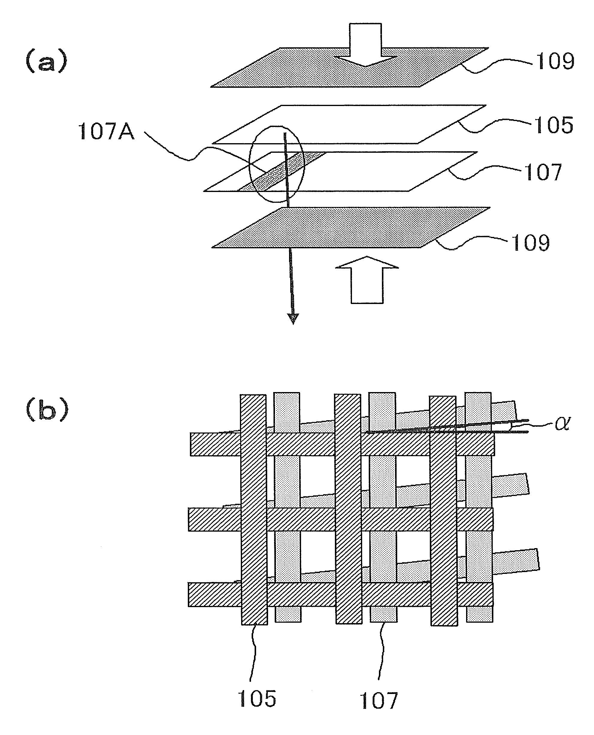
[0204]In Examples 2 to 7, a fibrous base material was prepared using the materials and the process as described in Example 1, but a misalignment angle was formed differently from Example 1. The fibrous base materials in Examples 2 to 7 had a bowing region where a smaller crossing angle of warps and wefts in the fibrous base material was less than 90°, and each example had a different misalignment angle.

[0205]

TABLE 3Ex. 2Ex. 3Ex. 4Ex. 5Ex. 6Ex. 7Misalignment angle (°)1.00.51.50.72.02.0

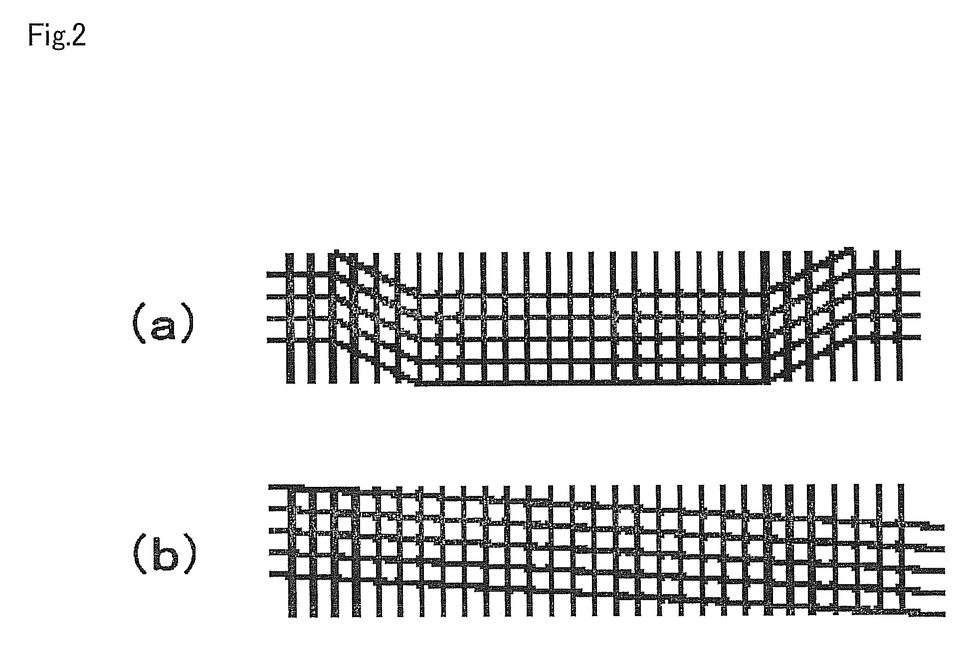
[0206]Furthermore, laminated bodies with a copper foil having different misalignment degrees were prepared as described in Example 1-(3). There were provided six laminated bodies with a copper foil having a misalignment degree of 0.0 ° to 1.5 ° . The laminated bodies with a copper foil thus prepared were etched to form a mesh pattern on the copper foil as described in Example 1.

[0207]Each of the six laminated bo...


PUM

PropertyMeasurementUnit
crossing angleaaaaaaaaaa
angleaaaaaaaaaa
thicknessaaaaaaaaaa

Abstract

There is provided a laminated body comprising a first resin layer consisting of a first fibrous base material and a resin and a second resin layer consisting of a second fibrous base material and a resin, wherein the first resin layer and the second resin layer are disposed such that the first resin layer and the second resin layer are at least partly positioned in separate regions separated by the center line in a thickness direction of the laminated body; wherein at least one of the first fibrous base material and the second fibrous base material has a bowing region where a bowing region is a region in which a smaller warp / weft crossing angle is less than 90° in the fibrous base material; and wherein in the bowing region, an angle formed by a warp of the first fibrous base material and a warp of the second fibrous base material and an angle formed by a weft of the first fibrous base material and a weft of the second fibrous base material, whichever is larger, is 2° or less.

Description

TECHNICAL FIELD[0001]The present invention relates to a laminated body, a circuit board with a laminated body, a semiconductor package and a process for manufacturing a laminated body.BACKGROUND ART[0002]Recent requirements for higher functions and reduction in a weight and a size in electronics have accelerated high-density integration and high-density mounting of electronic components. There is, however, a problem that a highly multilayered structure associated with high-density integration and mounting leads to increase an overall thickness of a multilayer printed wiring board. Thus, there has been devised a technique that a thinner glass cloth or resin layer is employed to make a core substrate thinner.[0003]A core base material of a common semiconductor package is a laminated body including a plated material prepared by impregnating a fibrous base material (for example, a glass cloth) with a resin and semi-curing (so-called prepreg). Currently-used core materials predominantly ...

Claims


Application Information

Patent Timeline
Patent Type & Authority Patents(United States)
IPC IPC(8): D03D13/00B32B5/12B32B15/14B32B5/08H05K1/02B32B5/28D04H13/00B32B27/38B29C65/00H05K1/03B32B5/26
CPCB32B5/26H05K1/036H05K2201/029H05K1/0366H05K2201/09136B32B5/12B32B5/28H05K1/0271Y10T442/3463Y10T442/3415Y10T442/2951Y10T442/3179Y10T442/3431Y10T442/3301Y10T156/10Y10T442/3496Y10T428/24124B32B5/024B32B5/22B32B15/14B32B15/18B32B15/20B32B27/12B32B27/281B32B27/304B32B27/32B32B27/322B32B27/36B32B29/005B32B29/02B32B2260/021B32B2260/028B32B2260/046B32B2262/02B32B2262/0261B32B2262/0269B32B2262/0276B32B2262/101B32B2307/30B32B2307/50B32B2307/54B32B2307/718B32B2457/08B32B5/10
Inventor YOSHIZAKI, KAZUYUKIITO, TEPPEIONOZUKA, IJINAKAMURA, KENSUKE
Owner SUMITOMO BAKELITE CO LTD
Why Eureka
Try Eureka