Method of forming metal oxide hardmask

a metal oxide and hardmask technology, applied in the field of metal oxide hardmask and spacer film, can solve the problems of unexpected critical dimension (cd) changes, difficulty in forming patterns with pitches, and insufficient lt-sio etching, etc., and achieve the effect of rapid degradation

Active Publication Date: 2014-12-02
ASM JAPAN
View PDF22 Cites 392 Cited by
  • Summary
  • Abstract
  • Description
  • Claims
  • Application Information

AI Technical Summary

Benefits of technology

[0021]An embodiment of the present invention provides a method of forming a metal oxide hardmask on a template, comprising: (i) providing a template constituted by a photoresist or amorphous carbon formed on a substrate; and (ii) depositing by atomic layer deposition (ALD) a metal oxide hardmask on the template constituted by a material having a formula SixM(1-x)Oy wherein M represents at least one metal element, x is less than one including zero, and y is approximately two or a stoichiometrically-determined number. The “hardmask” refers to a material used in any semiconductor processing as an etch mask in lieu of polymer or other organic “soft” materials (target films) which tend to be etched easily by oxygen, fluorine, chlorine, or other reactive gases to the extent that a pattern defined using the “soft” mask can be rapidly degraded during plasma etching as compared with the hardmask.

Problems solved by technology

Photolithography technology has recently faced difficulty of forming patterns having pitches smaller than the submicron level.
However, the LT-SiO does not have sufficient etch (dry and / or wet) selectivity relative to a base film, thereby causing unexpected critical dimension (CD) changes or the like.
Otherwise, the template may be damaged by heat during the deposition of the spacer film, and additionally, if the temperature is as high as 400° C., diffusion or migration of Cu or B into a device such as an insulation film, wiring, or transistor may occur.
Conventional spacer films do not satisfy the above criteria.
Additionally, a metal such as V or Nb which is not commonly used in the semiconductor processing processes may not be a good candidate.
Many groups have studied conformal SiN deposition, but their attempts have not yet been successful to provide a solution to obtaining conformal SiN film.
In step (d), the exposed PR 2′ is removed by etching, and as a result, the spacer 3′ collapses, deteriorating the pattern.
However, it is very difficult to maintain hydrophobicity of the surface of the spacer for SDDP because even if the hydrophobic material is used, after ashing (typically by exposing the template to an oxidant plasma such as an oxygen plasma, N2O plasma, and CO2 plasma, the surface is easily changed to hydrophilic because hydrophilic O—H is easily generated on the oxidized surface after air exposure.

Method used


Image

  • Method of forming metal oxide hardmask
  • Method of forming metal oxide hardmask
  • Method of forming metal oxide hardmask

Examples


example

Example 1

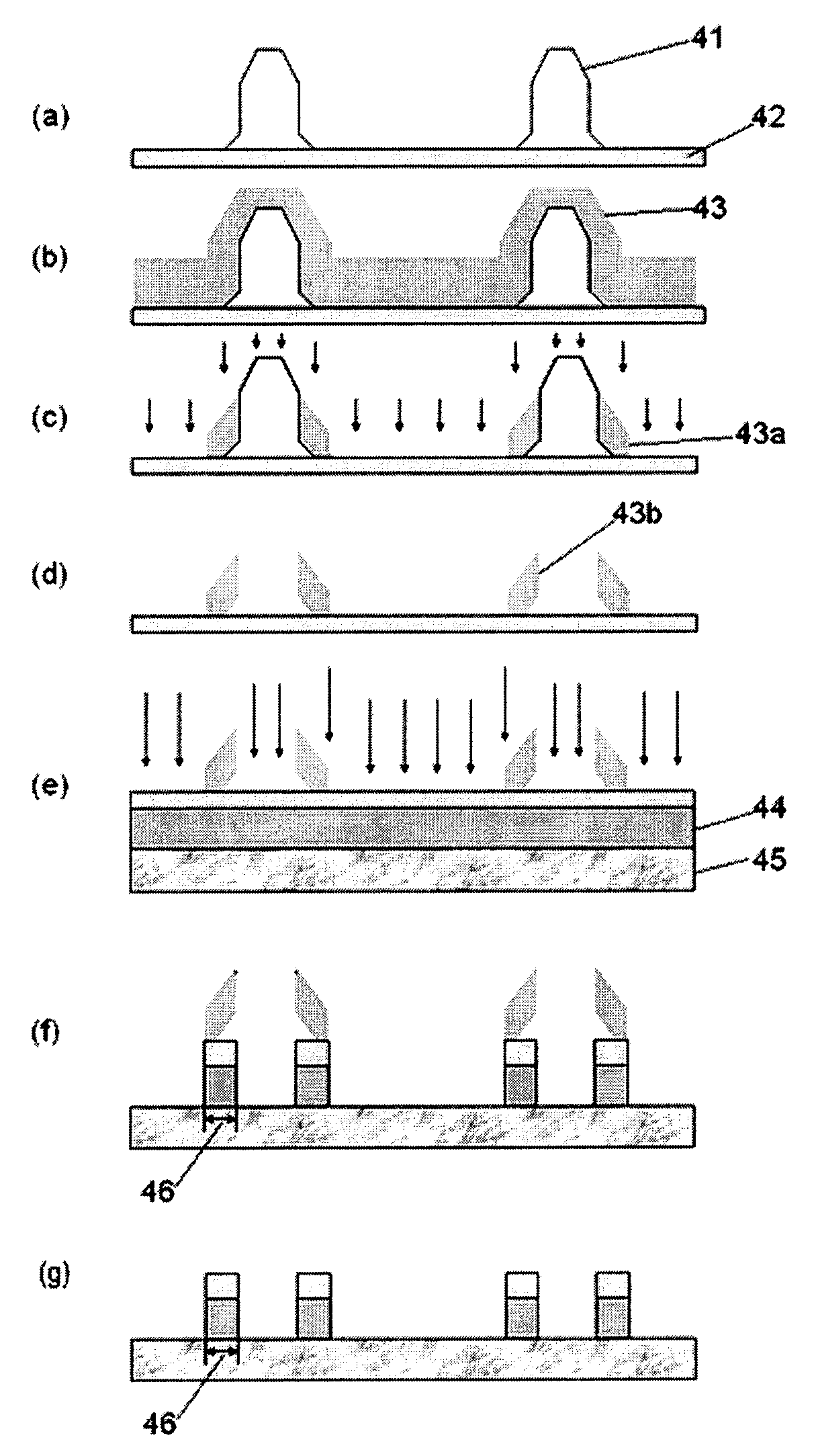
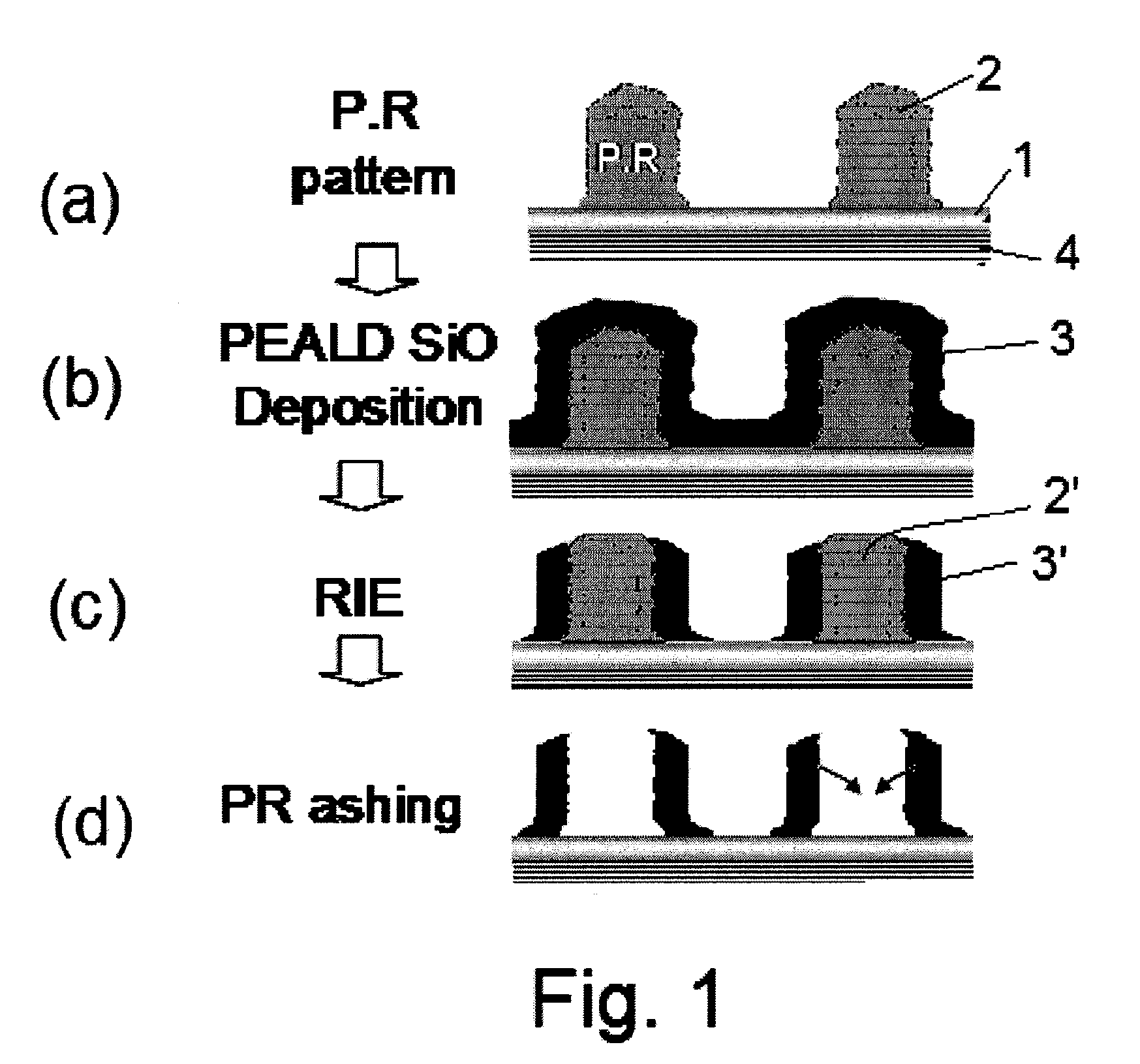
[0072]A metal oxide hardmask film was formed on a substrate (Φ200 mm) by PE-ALD under the conditions shown below using the PE-ALD apparatus illustrated in FIG. 6. The sequence in each cycle of PE-ALD is shown in FIG. 7.

[0073]

TABLE 1PrecursorTitanium tetra-isopropoxideDeposition temperature50deg C.Reactant gas flowO2, 500sccmCarrier gas flowAr, 2000sccmDeposition pressure200PaRF power (27.12 MHz)50WDeposition process sequenceStep 1:Step 2:Step 3:Step 4:Precursor feedPrecursor purgeRF ignitionPost purge0.9 sec2.0 sec0.5 sec0.5 sec

[0074]A SiO hardmask (LT-SiO) was also formed on a substrate by PE-ALD under conditions substantially the same as above.

[0075]Dry etch selectivity and wet etch selectivity of each hardmask (also those of standard thermal oxide) were measured, and the results are shown below.

[0076]

TABLE 2ThermaloxidePEALD LT-SiOPEALD TiO2Dry etch rate0.201.000.11(NF3, 100 deg C.)Wet etch rate0.091.000.10(DHF 1:100)

[0077]Hardness and Elastic modulus of each hardmask we...

example 2

[0080]In the same manner as described in Example 1 except for the conditions shown in Table 4 below, films were deposited to compare film growth rates using titanium tetraisopropoxide (TTIP) and tetrakis-dimethylaminotitanium (TDMAT). As can be seen from the table, the film growth rate by TDMAT was nearly two times higher (2-3, 2-4) than that by TTIP (2-1, 2-2). The properties of the obtained film by TDMAT were comparable with those by TTIP, although the wet etch rate of the film by TDMAT was increased by about two to three times that by TTIP. Additionally, by prolonging the RF ignition time (2-5), the mechanical strength was increased and the wet etch rate was reduced.

[0081]

TABLE 42-12-22-32-42-5PrecursorTTIPTTIPTDMATTDMATTDMATRF power50 W100 W50 W100 W100 WRF ignition time per cycle0.4 sec0.4 sec0.4 sec0.4 sec2.0 secGPC(nm / cycle)0.0420.0420.0790.0740.059RI2.4012.4072.2812.3082.415WER (1:100 DHF)Ratio0.750.842.791.470.64compared tothermal oxideHardness(GPa)9.019.398.108.9012.70EM(G...

example 3

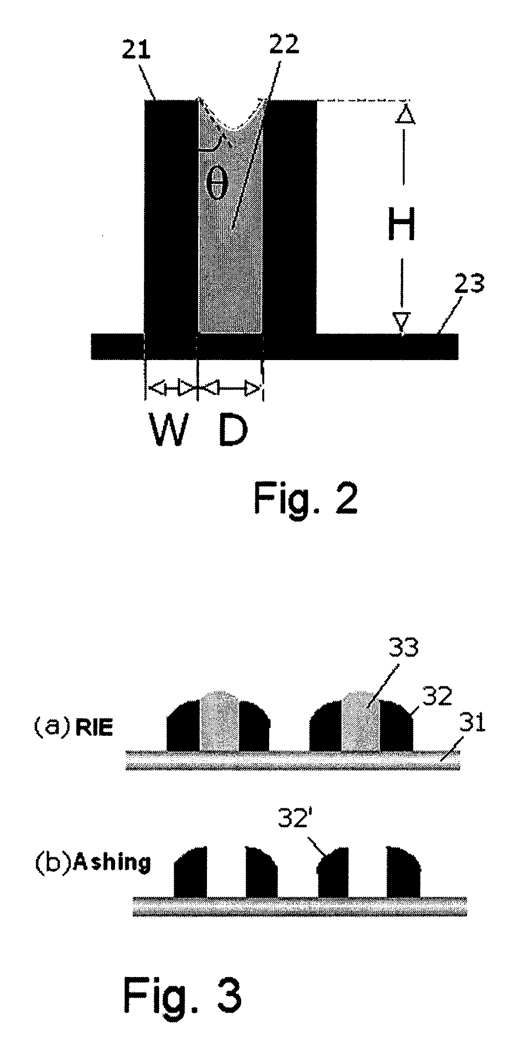
[0082]In the same manner as described in Example 1 except for the conditions shown in Tables 5 and 6 below, films were deposited to confirm controllability of film stress. As can be seen from Table 6, the film stress was well controlled by changing plasma-on time (duration of RF ignition) and / or plasma power (RF power), indicating that the films obtained using TTIP are suitable as a spacer having pattern-collapsing resistance. That is, by increasing the plasma-on time, the degree of tensile stress of the film can be reduced, and by increasing plasma power, the degree of tensile stress of the film can be reduced and can even be changed to compressive stress.

[0083]

TABLE 5TiO2SourceTTIP 23 sccmReactant gasOxygen 500 sccmCarrier gasAr2000 sccmPressure200 PaRF powerVariable (X) WSource feedPurge 1Plasma onPurge 20.3 sec 0.6 secVariable (Y) sec0.1 sec

[0084]

TABLE 6ProcessPrecursorPlasma powerPlasma-ontemperaturesupply(X)time (Y)Film stress100 deg C.TTIP 50 W0.4 sec+388 MPa100 deg C.TTIP 50...


PUM

PropertyMeasurementUnit
vapor pressureaaaaaaaaaa
temperatureaaaaaaaaaa

Abstract

A method of forming a metal oxide hardmask on a template includes: providing a template constituted by a photoresist or amorphous carbon formed on a substrate; and depositing by atomic layer deposition (ALD) a metal oxide hardmask on the template constituted by a material having a formula SixM(1-x)Oy wherein M represents at least one metal element, x is less than one including zero, and y is approximately two or a stoichiometrically-determined number.

Description

CROSS-REFERENCE TO RELATED APPLICATIONS[0001]This application claims the benefit of U.S. Provisional Application No. 61 / 427,661, filed Dec. 28, 2010 under 35 USC 119(e), the disclosure of which is herein incorporated by reference in its entirety.BACKGROUND[0002]The present invention relates to semiconductor integrated circuit manufacturing and, more particularly to a method of forming a hardmask, particularly a spacer film.DESCRIPTION OF THE RELATED ART[0003]Photolithography technology has recently faced difficulty of forming patterns having pitches smaller than the submicron level. Various approaches have been studied, and one of the promising methods is space-defined double patterning (SDDP) which makes it possible to create narrow pitches beyond limitations of conventional lithography such as light source wavelength and high index immersion fluid. Generally, SDDP needs one conformal spacer film and hardmask template wherein the conformal spacer film is deposited on the template n...

Claims


Application Information

Patent Timeline
Patent Type & Authority Patents(United States)
IPC IPC(8): H01L21/033H01L21/228H01L21/02
CPCH01L21/0337H01L21/02274H01L21/02153H01L21/02186H01L21/0228G03F1/00H01L21/0215H01L21/02164H01L21/02172H01L21/02554
Inventor HA, JEONGSEOKFUKUDA, HIDEAKIKAIDO, SHINTARO
Owner ASM JAPAN
Why Eureka
Try Eureka