Conductive polymer compositions in opto-electrical devices

a technology of opto-electrical devices and conductive polymer compositions, which is applied in the direction of conductive materials, organic conductors, non-conductive materials with dispersed conductive materials, etc., can solve the problems of lateral conduction and shorting between electrodes, poor performance, and many significant problems, and achieve the effect of more viscosity and thinness

Inactive Publication Date: 2015-02-03
CAMBRIDGE DISPLAY TECH LTD +1
View PDF57 Cites 17 Cited by
  • Summary
  • Abstract
  • Description
  • Claims
  • Application Information

AI Technical Summary

Benefits of technology

[0027]Preferably, the conductive polymer comprises a conductive polymer ion and the conductive polymer composition further comprises a counter ion. Conductive polymer ions have been found to be good conductors and the counter ions aid in stabilizing the conductive polymer ions.
[0069]The addition of polyethylene glycol enables the resistivity of the conductive polymer to be tuned to a desired value. Preferably, polyethylene glycol having a molecular weight of 250 is added to a PEDOT composition in the range 0 to 3% concentration by weight, preferably 1 to 3%, more preferably, 1 to 2%, most preferably less than or equal to 1.5% and very preferably less then 1.25%.

Problems solved by technology

However, there are several significant problems.
For example, if a plurality of electrodes are provided in a device but only one continuous layer of conductive polymer extending over all the electrodes, then too high a conductivity can lead to lateral conduction and shorting between electrodes.
However, it was found that small counter ions migrated though the system when subjected to an electromagnetic field causing charge separation and charge build up in localized areas / interfaces of a device resulting in poor performance.
Migration of the counter ion can also lead to adverse reactions with materials in adjacent layers.
It has been found that varying the ratio of PEDOT:PSS in a layer of a device significantly changes the functional performance of the device.
However, at a ratio of 1:2.5 the conductivity is very high and as such this material cannot be used in some opto-electronic device arrangements as it can, for example, short connections between electrode lines in a device as discussed previously.
Without being bound by theory, one possible limitation on the lifetime of devices using the aforementioned PEDOT-PSS system is that the provision of such a large excess of PSS results in a composition which is very acidic.
This may cause several problems.
Furthermore, the acid may interact with light emitting polymers resulting in charge separation which is detrimental to device performance.
This can take anything between a few seconds and a few minutes to dry and results in a relatively thin film in comparison with the initial “ink” volume.

Method used


Image

  • Conductive polymer compositions in opto-electrical devices
  • Conductive polymer compositions in opto-electrical devices
  • Conductive polymer compositions in opto-electrical devices

Examples


Embodiment Construction

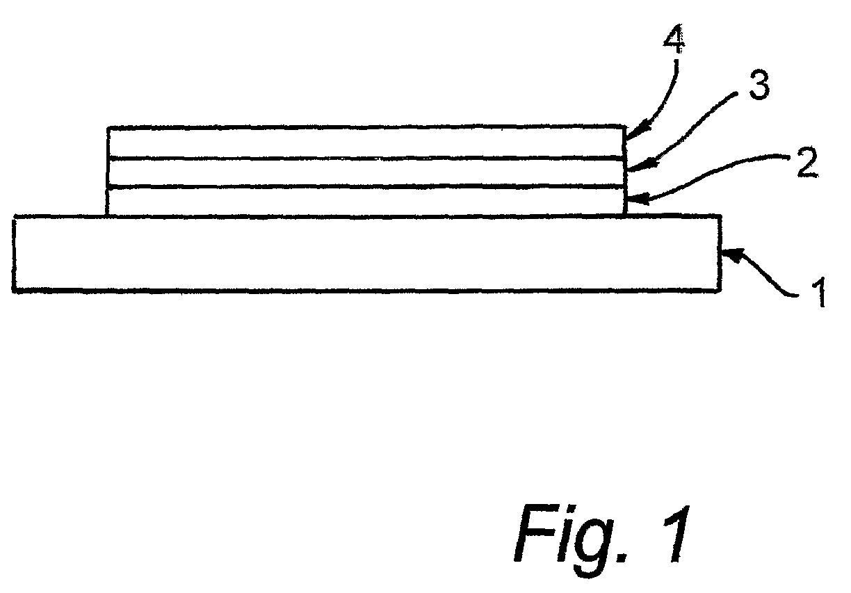
[0086]The device shown in FIG. 1 comprises a transparent glass or plastic substrate 1, an anode 2 of indium tin oxide and a cathode 4. An electroluminescent layer 3 is provided between anode 2 and cathode 4.

[0087]Further layers may be located between anode 2 and cathode 3, such as charge transporting, charge injecting or charge blocking layers.

[0088]In accordance with an embodiment of the present invention, a conductive hole injection layer formed of a conductive polymer composition is located between the anode 2 and the electroluminescent layer 3 to assist hole injection from the anode into the layer or layers of semiconducting polymer.

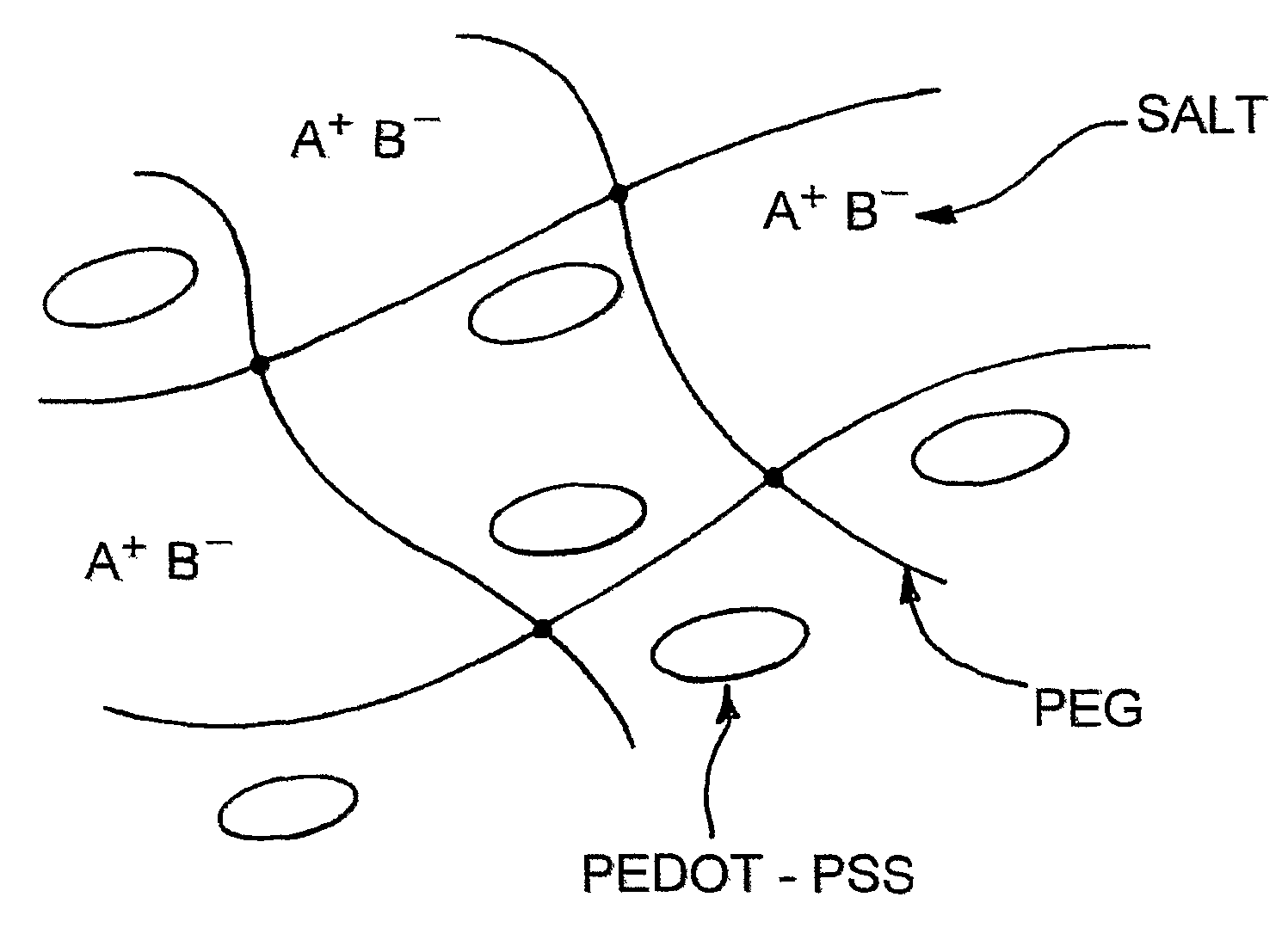
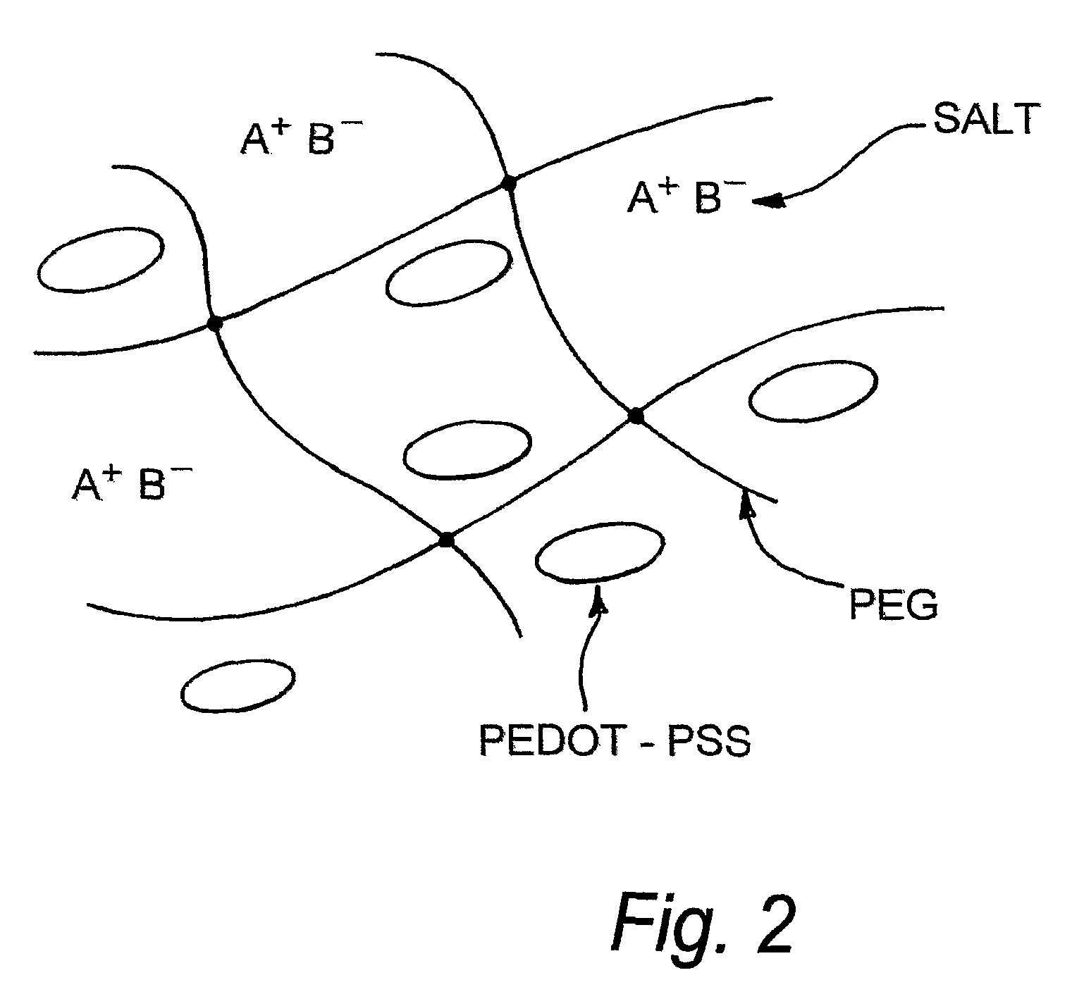
[0089]The hole injection layer may be made by mixing PEDOT:PSS at a ratio of 1:2.5 with PEG and lithium triflimide in water. The resultant composition may be spin coated or ink jet printed to form a layer on the anode. The layer may then be heated to thermally cross-link the polyelectrolyte matrix after deposition. A schematic diagram illustrated the...


PUM

PropertyMeasurementUnit
work functionaaaaaaaaaa
sheet resistanceaaaaaaaaaa
ionisation potentialaaaaaaaaaa

Abstract

A conductive polymer composition comprising a conductive polymer in a solid polyelectrolyte.

Description

FIELD OF INVENTION[0001]This invention relates to conductive polymer compositions and opto-electrical devices comprising conductive polymer compositions.BACKGROUND OF INVENTION[0002]One class of opto-electrical devices is that using an organic material for light emission or detection. The basic structure of these devices is a light emissive organic layer, for instance a film of a poly (p-phenylenevinylene) (“PPV”) or polyfluorene, sandwiched between a cathode for injecting negative charge carriers (electrons) and an anode for injecting positive charge carriers (holes) into the organic layer. The electrons and holes combine in the organic layer generating photons. In WO90 / 13148 the organic light-emissive material is a polymer. In U.S. Pat. No. 4,539,507 the organic light-emissive material is of the class known as small molecule materials, such as (8-hydroxyquinoline)aluminium (“Alq3”). In a practical device one of the electrodes is transparent, to allow the photons to escape the devi...

Claims


Application Information

Patent Timeline
Patent Type & Authority Patents(United States)
IPC IPC(8): H01B1/06H01B1/24C08L65/00C08L71/02C09D11/00C09D11/30H01B1/12
CPCH01B1/127C08L65/00C09D11/30H01B1/122C08L71/02C08L71/00Y10T428/24802Y10T29/49115
Inventor TOWNS, CARL R.HOLMES, ANDREW BRUCEMCKIERNAN, MARY J.
Owner CAMBRIDGE DISPLAY TECH LTD
Why Eureka
Try Eureka