Semiconductor device with ONO film

a technology of ono film and semiconductor, applied in the field of semiconductor devices, can solve the problems of difficult to distinguish the electrons stored in the area from each other, the f-n tunnel effect cannot be practically applied for data erasure, and the difficulty of high integration and miniaturization of memory cells, so as to reduce the amount of electrons accumulated in the trap layer in the middle between the bit lines, the effect of suppressing the interference of electrons accumulated in the charge storage area and reducing the amount of electron

Active Publication Date: 2015-03-31
LONGITUDE FLASH MEMORY SOLUTIONS LTD
View PDF7 Cites 3 Cited by
  • Summary
  • Abstract
  • Description
  • Claims
  • Application Information

AI Technical Summary

Benefits of technology

[0009]According to an aspect of the present invention, there is provided a semiconductor device including: a semiconductor substrate; bit lines provided in the semiconductor substrate; an ONO film that is provided along a surface of the semiconductor substrate and includes a tunnel oxide film, a trap layer made of a nitride film, and a top oxide film; and an oxide film that is provided on the surface of the semiconductor substrate in a middle portion between the bit lines along the surface of the semiconductor substrate and contacts a side face of the ONO film. The film thickness of the oxide film is larger than the sum of the thicknesses of the tunnel oxide film and the top oxide film, and smaller than the thickness of the ONO film. According to the present invention, interference of electrons accumulated in a charge storage area can be suppressed, and electrons can be removed from a charge storage layer by the F-N tunnel effect. Therefore, high integration and miniaturization of memory cells become possible.
[0010]According to another aspect of the present invention, there is provided a semiconductor device including: a semiconductor substrate; bit lines provided in the semiconductor substrate; and an ONO film that is provided along a surface of the semiconductor substrate and includes a tunnel oxide film, a trap layer made of a nitride film, and a top oxide film. The film thickness of the trap layer in a middle portion between the bit lines along the surface of the semiconductor substrate is smaller than the thickness of the trap layer in portions in contact with the bit lines. According to this aspect of the present invention, the amount of electrons accumulated in the trap layer in the middle between the bit lines can be reduced. Therefore, interference of electrons accumulated in a charge storage area can be mitigated.
[0011]According to yet another aspect of the present invention, there is provided a manufacturing method of a semiconductor device including: forming bit lines in a semiconductor substrate; forming along a surface of the semiconductor substrate an ONO film that includes a tunnel oxide film, a trap layer made of a nitride film, and a top oxide film; etching the top oxide film in a middle portion between the bit lines along the surface of the semiconductor substrate; and oxidizing the trap layer under a portion where the top oxide film is etched. According to this aspect of the present invention, it is easy to form in the middle between the bit lines an oxide film whose thickness is larger than the sum of the thicknesses of the tunnel oxide film and the top oxide film and smaller than the thickness of the ONO film.
[0012]According to a further aspect of the present invention, there is provided a manufacturing method of a semiconductor device including: forming on a surface of a semiconductor substrate an ONO film that includes a tunnel oxide film, a trap layer made of a nitride film, and a top oxide film; forming a mask layer on the ONO film; forming bit lines in the semiconductor substrate using the mask layer as a mask; forming on the bit lines an insulating film that is penetrating the ONO film, defined by the mask layer, and thicker than the ONO film; etching the top oxide film using as a mask a first sidewall layer provided on a sidewall of the insulating film on the ONO film; and oxidizing the trap layer under a portion where the top oxide film is etched. According to this aspect of the present invention, it is possible to form an oxide film self-aligned to the bit lines whose thickness is larger than the sum of the thicknesses of the tunnel oxide film and the top oxide film and smaller than the thickness of the ONO film.

Problems solved by technology

As a result, it becomes difficult to distinguish the electrons stored in the areas from each other (that is, to read data distinctly).
Therefore basically, the F-N tunnel effect cannot be practically applied for data erasing.
As described above, the related-art example has a problem that it is difficult to highly densify and miniaturize memory cells.

Method used


Image

  • Semiconductor device with ONO film
  • Semiconductor device with ONO film
  • Semiconductor device with ONO film

Examples


first embodiment

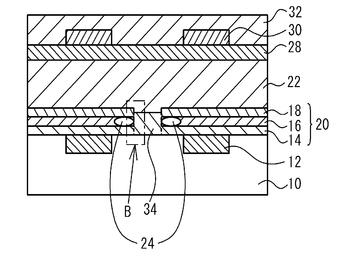
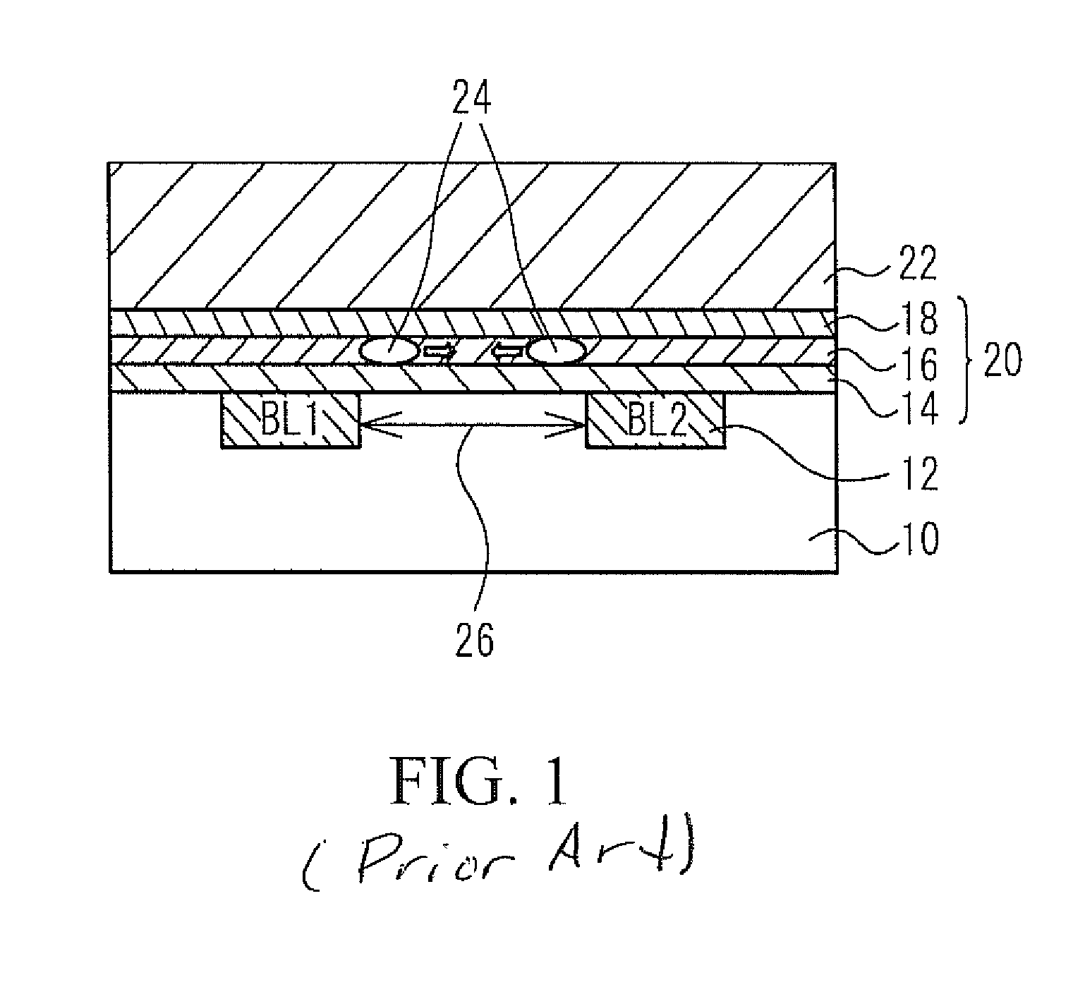
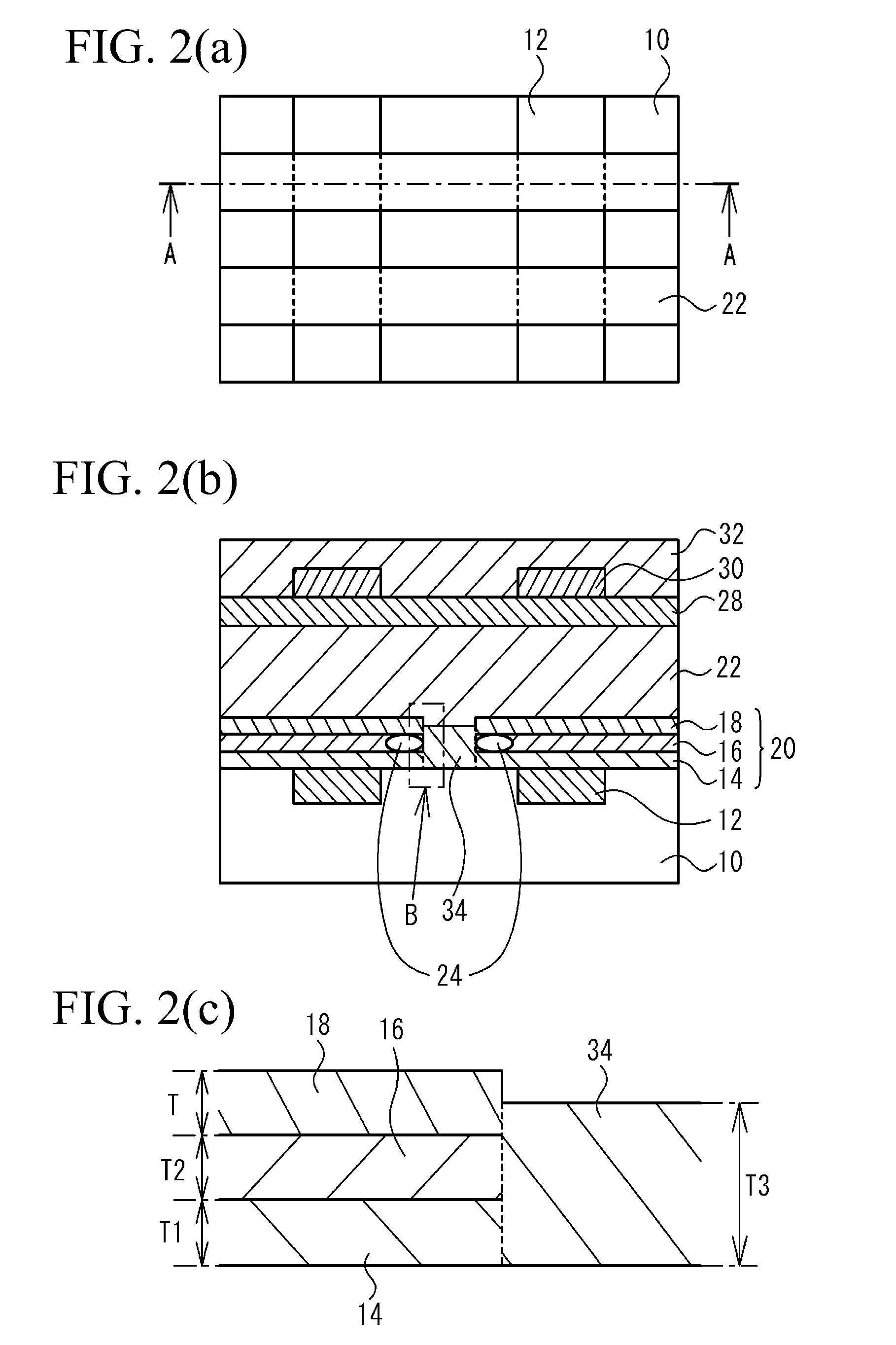
[0036]FIG. 2(a) is an upper plan view of a flash memory according to a first embodiment, and FIG. 2(b) is a cross-sectional view taken along A-A in FIG. 2(a). FIG. 2(c) is an enlarged view of an area B in FIG. 2(b). Note that in FIG. 2(a), illustration of an interlayer insulating film 28, a wiring layer 30, a protection film 32, an ONO film 20, and an oxide film 34 is omitted. FIG. 3(a) is a cross-sectional view of a flash memory according to a comparative example in the place corresponding to section A-A in FIG. 2(a), and FIG. 3(b) is an enlarged view of area B in FIG. 3(a). With reference to FIG. 2(a), the flash memory according to the first embodiment is provided in its semiconductor substrate 10, which is a p-type silicon substrate (or a semiconductor substrate with a p-type silicon area), with a bit line 12, which is made of an n-type diffusion layer and serves as both the source and the drain, and a word line 22, which is made of, for example, a polysilicon film and serves als...

second embodiment

[0058]FIG. 14 is a cross-sectional view of a flash memory according to a second embodiment in the place corresponding to section A-A in FIG. 2(a). With reference to FIG. 14, on the bit line 12 is provided an insulating film 38 that penetrates the ONO film 20 and has a film thickness larger than that of the ONO film 20. The word line 22 is provided so as to cover the insulating film 38 and to contact the ONO film 20. Since the other configuration is the same as that of the first embodiment and shown in FIG. 2(a) to FIG. 2(c), its description is omitted.

[0059]Next, using FIG. 15(a) to FIG. 16(c), a manufacturing method of the flash memory according to the second embodiment is described. With reference to FIG. 15(a), on the semiconductor substrate 10 are sequentially formed the tunnel oxide film 14 made of a silicon oxide film, the trap layer 16 made of a silicon nitride film, and the top oxide film 18 made of a silicon oxide film. In this way is formed the ONO film 20 on the semicondu...

third embodiment

[0067]FIG. 19 is a cross-sectional view of a flash memory according to a third embodiment in the place corresponding to section A-A in FIG. 2(a). With reference to FIG. 19, in the semiconductor substrate 10 between the bit lines 12 provided in the semiconductor substrate 10, a groove portion 44 is provided. Along the inner surface of the groove portion 44 is provided an ONO film 20, and on the bottom face of the groove portion 44 is provided the oxide film 34. By the oxide film 34 provided on the bottom face of the groove portion 44, the trap layer 16 is separated. Since the other configuration is the same as that of the first embodiment and shown in FIG. 2(a) to FIG. 2(c), its description is omitted.

[0068]Next, using FIG. 20(a) to FIG. 20(c), a manufacturing method of the flash memory according to the third embodiment is described. Since the process to form the bit line 12 in the semiconductor substrate 10 is the same as those of the first embodiment and shown in FIG. 5(a), its des...


PUM


Abstract

A semiconductor device includes bit lines provided in a semiconductor substrate; an ONO film that is provided along the surface of the semiconductor substrate and is made of a tunnel oxide film, a trap layer, and a top oxide film; and an oxide film that is provided on the surface of the semiconductor substrate in the middle between the bit lines and contacts the side face of the ONO film, in which the film thickness of the oxide film is larger than the sum of the thicknesses of the tunnel oxide film and the top oxide film, and smaller than the thickness of the ONO film.

Description

CROSS-REFERENCE TO RELATED APPLICATIONS[0001]The present invention is based on Japanese Patent Application No. 2007-067151 filed on Mar. 15, 2007, the entire disclosure of which is hereby incorporated by reference.TECHNICAL FIELD[0002]The present invention relates to a semiconductor device and its manufacturing method, and more particularly to a semiconductor device provided with a nonvolatile memory in which each transistor has two charge storage areas, as well as its manufacturing method.BACKGROUND ART[0003]In recent years, nonvolatile memories, which are semiconductor devices that keep stored data even if the power is turned off, are widely used. In a flash memory, which is a typical nonvolatile memory, each transistor constituting a memory cell has a floating gate or an insulating film called a charge storage layer. Data storage is performed by storing electrons in such charge storage layers. As a flash memory having a charge storage layer formed of an insulating film, there is ...

Claims


Application Information

Patent Timeline
Patent Type & Authority Patents(United States)
IPC IPC(8): H01L29/792H01L21/28H01L27/115H01L29/423H01L29/51
CPCH01L29/511H01L21/28282H01L27/115H01L27/11568H01L29/42352H01L29/7923H01L2924/0002H01L29/40117H10B43/30H10B69/00H01L2924/00H01L21/02164H01L21/0217H01L21/0223H01L21/31111H01L21/31144H01L21/768H01L23/528H01L29/513H01L29/518
Inventor HAYAKAWA, YUKIOUTSUNO, YUKIHIRO
Owner LONGITUDE FLASH MEMORY SOLUTIONS LTD
Why Eureka
Try Eureka