Semiconductor memory device with a clock circuit for reducing power consumption in a standby state

a technology of memory device and clock circuit, which is applied in the field of semiconductor devices, can solve the problems of high-speed operation that is difficult to be implemented, extra power consumption, leakage current, etc., and achieves the effects of reducing the leakage current of the first mos transistor, high integration and miniaturization of the logic circuit, and fast processing

Active Publication Date: 2015-08-18
WINBOND ELECTRONICS CORP
View PDF19 Cites 10 Cited by
  • Summary
  • Abstract
  • Description
  • Claims
  • Application Information

AI Technical Summary

Benefits of technology

[0020]According to the above descriptions, in the standby state, the second operation voltage lower than the first operation voltage is supplied to the first MOS transistor. Therefore, compared to supply of the first operation voltage, the leakage current of the first MOS transistor is reduced. Moreover, the second operation voltage is set so that the voltage amplitude between the gate and the source of each of the first MOS transistor and the second MOS transistor is greater than the threshold of the first MOS transistor and the second MOS transistor. Therefore, a logic level of the signal input to the logic circuit is maintained. Accordingly, when the standby state is changed to the enable state, the logic circuit is unnecessary to be initialised to implement quick processing. Moreover, it is unnecessary to add a transistor logically set according to the power down signal to the logic circuit as that does of the conventional technique, so that high integration and miniaturization of the logic circuit can be implemented.

Problems solved by technology

In order to implement the above demands, some side effects are produced, for example, in fabrication of a single layer of polysillicon, increase of a threshold of a P-channel metal oxide semiconductor transistor may cause a side effect that a high-speed operation is hard to be implemented.
However, when the threshold is reduced, even if a voltage Vgs between a gate and a source of the transistor is 0V, a phenomenon of leakage current still exists, which may cause extra power consumption.
Generally, the smaller the threshold is, the larger the leakage current is, and the more obvious the power consumption is.
Moreover, in the standby state, since the output data is fixed to the high level, when the standby state is changed to the enable state, the logic portion has to be initialised, which takes more time for implementation.

Method used


Image

  • Semiconductor memory device with a clock circuit for reducing power consumption in a standby state
  • Semiconductor memory device with a clock circuit for reducing power consumption in a standby state
  • Semiconductor memory device with a clock circuit for reducing power consumption in a standby state

Examples


fifth embodiment

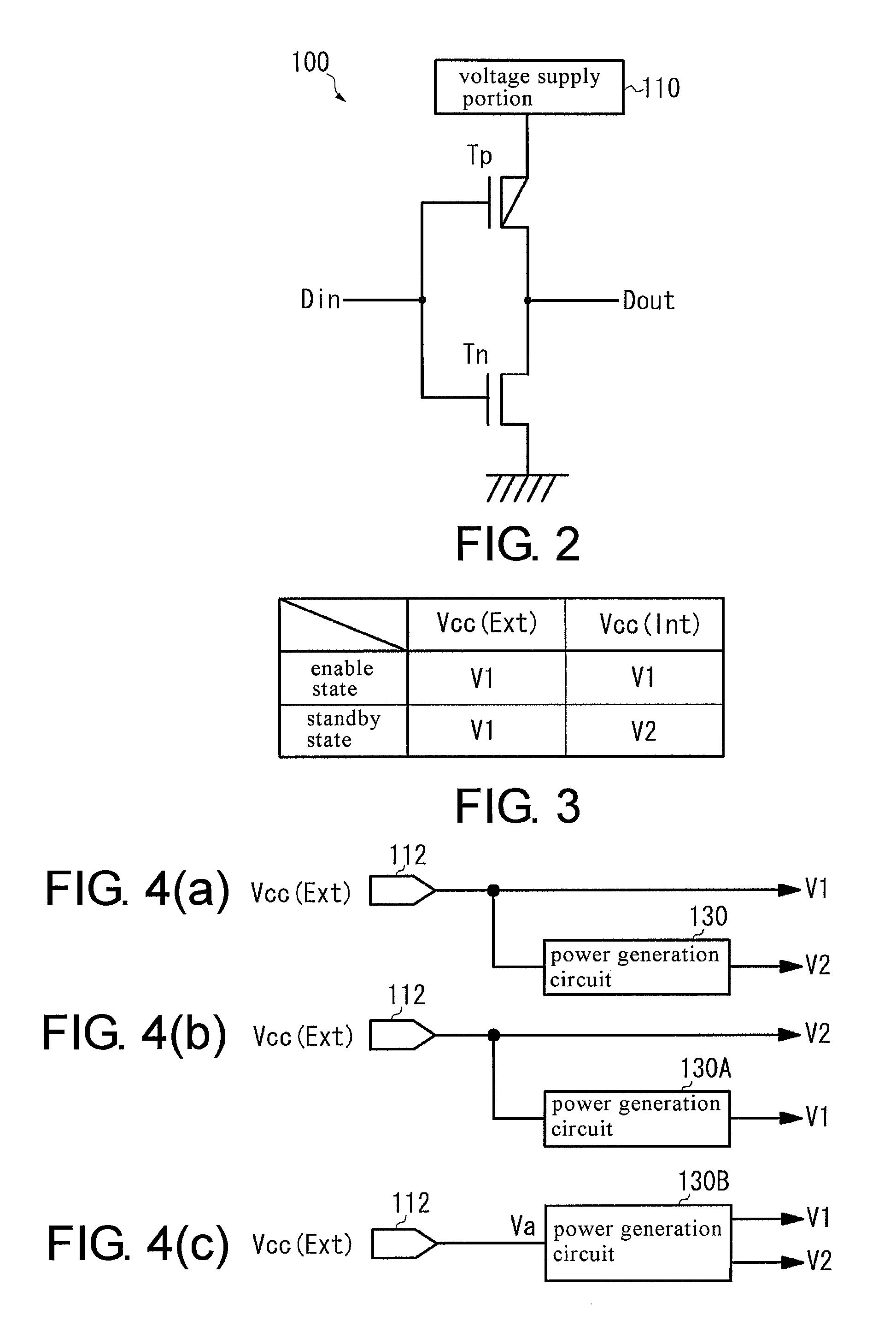
[0051]FIG. 8(b) is a circuit schematic diagram of an exemplary example of the logic circuit 170 of the The logic circuit 170 includes an inverter, a low-threshold P-channel transistor Tp, an N-channel transistor Tn, a low-threshold P-channel transistor Qp connected in series between the transistor Tp and the power supply portion 110, and an N-channel transistor Qn connected in series between the transistor Tn and the ground. The input data Din is input to the gates of the transistors Tp and Tn, the inverted internal clock signal InCLK is supplied to the gate of the transistor Qp, and the internal clock signal InCLK is supplied to the gate of the transistor Qn. In the enable state, the operation voltage V1 is supplied to the transistor Qp, the logic circuit 170 synchronously obtains the input data Din and the internal clock signal, and outputs the output data Dout.

[0052]In the standby state, the operation voltage V2 is supplied to the transistor Qp, and the leakage current of the tr...

sixth embodiment

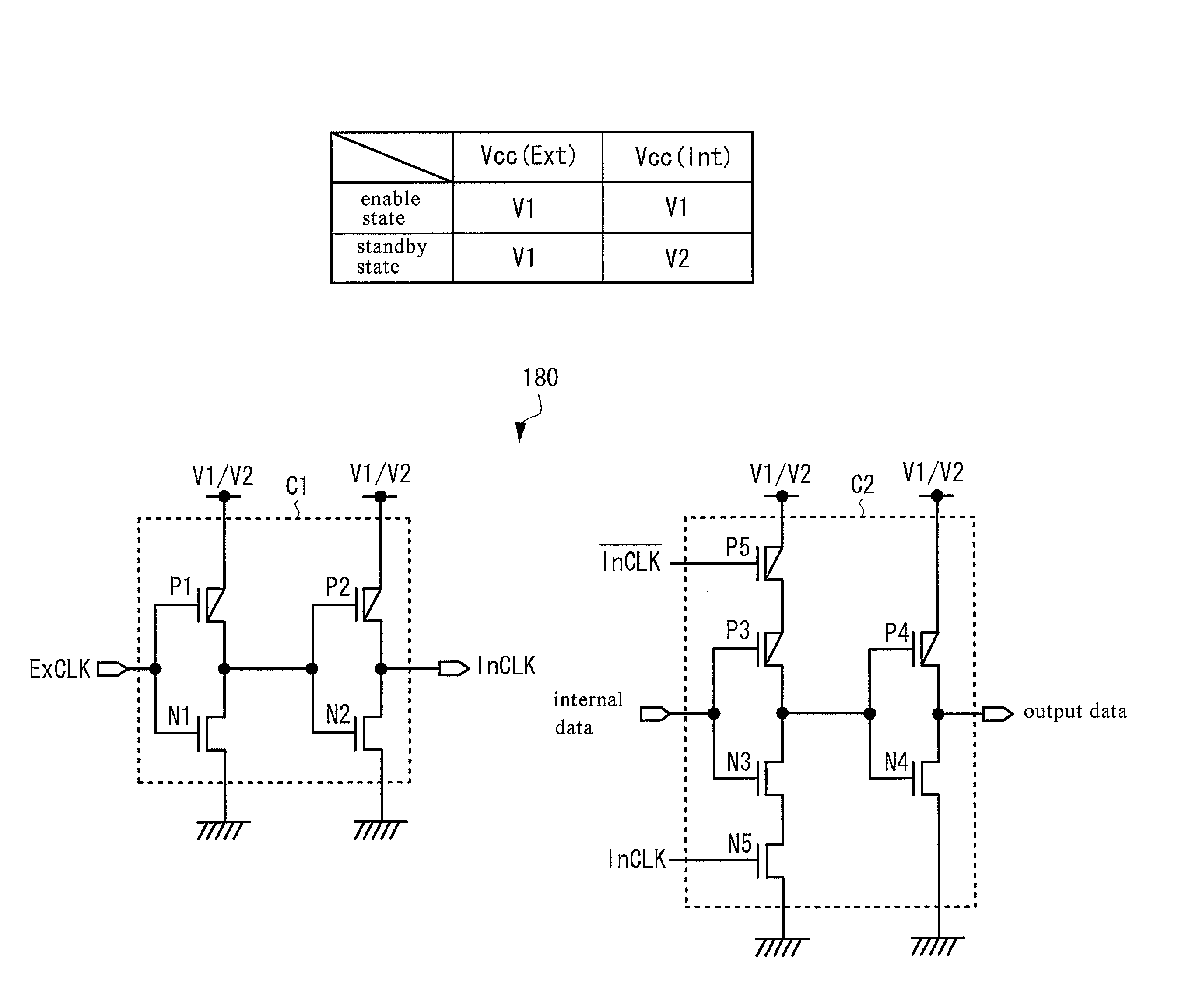
[0053]Then, referring to FIG. 9 to FIG. 12, circuit structures of a sixth embodiment are introduced below. FIG. 9 illustrates a data output circuit 180 according to the sixth embedment of the invention. The data output circuit 180 is, for example, adapted to an NAND flash memory 100E shown in FIG. 12. As shown in FIG. 12, the flash memory 100E includes a memory array 200, an input output buffer 210, an address register 220, a data register 230, a controller 240, a word line selector 250, a page buffer / sensing circuit 260, a row selector 270 and an internal voltage generation circuit 280.

[0054]The memory array 200 has a plurality of memory units arranged in a matrix. The input output buffer 210 is connected to an external input output terminal I / O and stores input output data. The address register 220 receives address data from the input output buffer 210. The controller 240 receives command data from the data register 230 or the input output buffer 210, and controls the devices acco...


PUM


Abstract

A semiconductor device including a logic circuit capable of decreasing a leakage current occurred during a standby state is provided. The semiconductor device includes a power supply portion for supplying a first operation voltage or a second operation voltage smaller than the first operation voltage; a P-type low-threshold transistor Tp for receiving the first or the second operation voltage from the power supply portion; and a N-type transistor Tn connected between the transistor Tp and a base potential. The transistors Tp, Tn construct a logic circuit. The power supply portion supplies the first operation voltage to the source of the transistor Tp in the enable state, and supplies the second operation voltage in a standby state. The second operation voltage is set so that voltage amplitude between gate and source of each transistor Tp, Tn is larger than the threshold value of the transistors Tp, Tn.

Description

CROSS-REFERENCE TO RELATED APPLICATION[0001]This application claims the priority benefit of Japan application serial no. 2011-106808, filed on May 12, 2011. The entirety of the above-mentioned patent application is hereby incorporated by reference herein and made a part of this specification.BACKGROUND OF THE INVENTION[0002]1. Field of the Invention[0003]The invention relates to a semiconductor device including a logic circuit or a logic gate. Particularly, the invention relates to a semiconductor device capable of reducing power consumption in a standby state.[0004]2. Description of Related Art[0005]Regarding memories such as flash memories and dynamic memories etc., according to demands of large capacity, low price and low power consumption, and small size fabrication steps thereof are also required to be simplified. In order to implement the above demands, some side effects are produced, for example, in fabrication of a single layer of polysillicon, increase of a threshold of a P...

Claims


Application Information

Patent Timeline
Patent Type & Authority Patents(United States)
IPC IPC(8): G11C7/10G11C7/22G11C5/14G11C16/30G11C16/20H03K19/00
CPCG11C5/147G11C5/148G11C7/1057G11C7/1084H03K19/0016G11C7/225G11C16/20G11C16/30G11C2207/2227G11C5/14G11C7/10G11C7/22
Inventor MURAKAMI, HIROKI
Owner WINBOND ELECTRONICS CORP
Why Eureka
Try Eureka