This helps you quickly interpret patents by identifying the three key elements:
Problems solved by technology
Method used
Benefits of technology
Benefits of technology
The present invention helps reduce the distance between different components and allows for more integrated and smaller module components to be obtained.
Problems solved by technology
On the other hand, in a soldering method for a surface mounting component, solder flash, explosion, distortion of the module substrate and reduction in dimensional accuracy due to preprocessing of the module substrate are likely to occur, and thus in view of such, a minimum inter-component distance of 0.15 mm is required.
However, in the process disclosed in Japanese Unexamined Patent Application Publication No. 2012-231182, the component built-in layer is obtained by curing epoxy resin or the like, and thus the component built-in layer warps after peeling the supporting body due to residual stress by the curing of resin.
Therefore, the coplanarity of the component built-in layer becomes unstable, and it becomes difficult to build up the insulating layer and the wiring layer on the surface of the component built-in layer.
Method used
Image
Click on the blue label to locate the original text in one second.
Reading with bidirectional positioning of images and text.
Examples
first embodiment
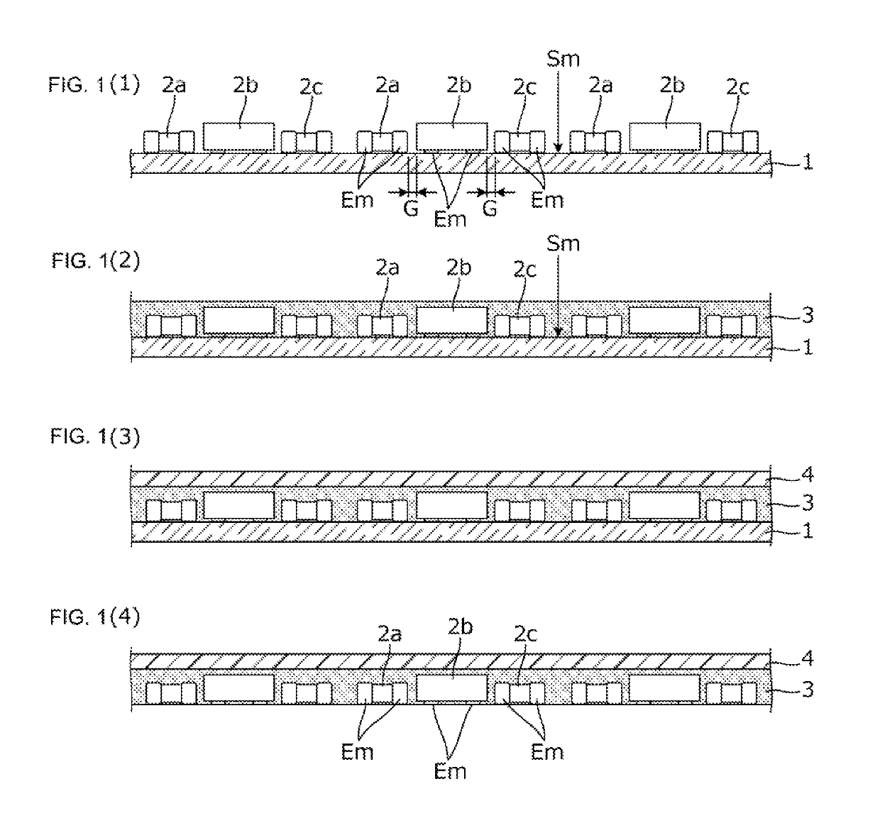
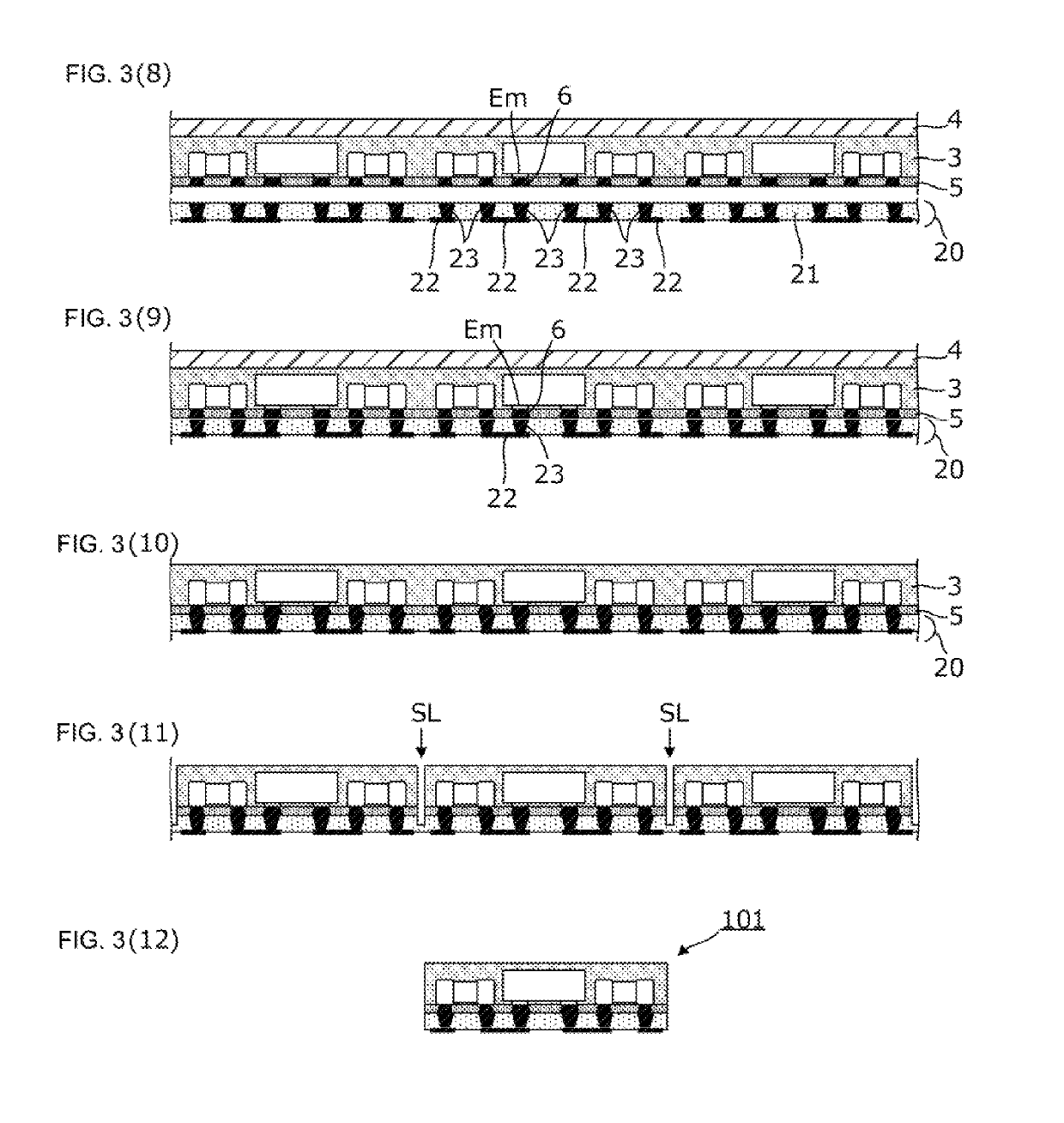
[0030]FIGS. 1, 2, and 3 are cross-sectional views of a substrate and each layer in each step of a twelve step method for manufacturing a module component according to a first embodiment (each successive step following the prior step). However, they are sectional views at a line not passing through each component, in which a cross section of each component does not appear.
[0031]Hereinafter, a method for manufacturing the module component 101 will be described in the order of these steps.
[0033]As shown in FIG. 1(1), surface mounting components 2a, 2b, 2c are arranged on a component mounting surface Sm of a transfer substrate 1. The surface mounting components 2a and 2c are preferably so-called dog-bone type chip components having a mounting terminal Em at both ends. The surface mounting component 2b is a semiconductorintegrated circuit component having an LGA type input / output terminal such as an IC chip that includes a mounting termin...
second embodiment
[0067]In a second embodiment, an example is shown in which the wiring sheet is configured by a stacked body of a plurality of the thermoplastic resin sheets.
[0068]FIGS. 7(1)-7(4) are cross-sectional views of a substrate and each layer in a predetermined step of the method for manufacturing a module component according to the second embodiment. The figure shows the step of joining the wiring sheet 20 to the resin layer 3 through the intermediate auxiliary layer 5, and the subsequent steps thereof. The steps before the steps shown in FIG. 7(1) are as shown in FIGS. 1(1) through 2(7) of the first embodiment.
[0069]As shown in FIGS. 7(1) and 7(2) of, a plurality of thermoplastic resin sheets 21 are overlapped with (placed in an overlapping positon with) the surface of the resin layer 3 on top of which the intermediate auxiliary layer 5 has been placed and heating and pressurizing are performed (heat treatment is performed), whereby the thermoplastic resin sheets 21 of the wiring sheet 20...
third embodiment
[0073]In a third embodiment, an example in which the configuration of the metal material formed in the openings H of the intermediate auxiliary layer 5 is different from that in the first and second embodiments is shown.
[0074]FIGS. 9(1) through 11(11) are cross-sectional views of a substrate and each layer in each step of the method for manufacturing the module component according to the third embodiment.
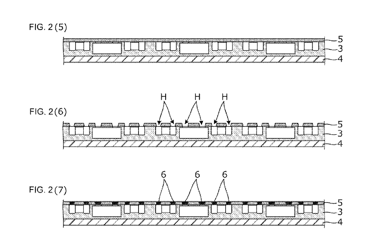
[0075]The steps shown in FIGS. 9(1)-9(4) and the steps shown in FIGS. 10(5) and 10(6) are the same as the steps shown in FIGS. 1(1)-1(4) and FIGS. 2(5) and 2(6) of the first embodiment. That is, [Surface mounting component burying step] [Warp preventing supporting material attaching step] and [Transfer substrate peeling step] are as shown in the first embodiment.
[0076]In the [Intermediate auxiliary layer processing step] of the present embodiment, a thin film of metal material 6 is formed in the openings H of the intermediate auxiliary layer 5, as shown in FIG. 10(7). For example, a...
PUM
Abstract
A plurality of surface mounting components are arranged on a component mounting surface of a transfer substrate. A resin layer is formed on the transfer substrate and the plurality of surface mounting components are buried in the resin layer. The resin layer is peeled off the transfer substrate, with the plurality of surface mounting components buried in the resin layer, to expose a surface resin layer. An intermediate auxiliary layer is provided on the exposed surface of the resin layer. The intermediate auxiliary layer has openings to expose respective mounting terminals of the surface mounting component. Metal materials are arranged in the openings. A wiring sheet which includes a thermoplastic resin sheet with an electrode pattern and a plurality of unmetallized via patterns is joined to the intermediate auxiliary layer so that each of the via patterns aligns with a respective one of the openings in the intermediate auxiliary layer. Heat treatment is performed to fuse the thermoplastic resin sheet to the intermediate auxiliary layer and to metallize the via patterns to connect the via patterns to the openings in the intermediate auxiliary layer and therefore the mounting terminals and the electrode pattern through the metal materials and the via patterns.
Description
CROSS REFERENCE TO RELATED APPLICATIONS[0001]The present application is a continuation of International application No. PCT / JP2017 / 028205, filed Aug. 3, 2017, which claims priority to Japanese Patent Application No. 2016-156908, filed Aug. 9, 2016, the entire contents of each of which are incorporated herein by reference.BACKGROUND OF THE INVENTIONField of the Invention[0002]The present invention relates to module components incorporated in an electronic device, and more particularly to a method for manufacturing a module component suitable for high integration or miniaturization.Description of the Related Art[0003]Various module components are generally configured by soldering a surface mounting component for configuring a predetermined circuit on a module substrate.[0004]Although miniaturization of each part of the constituent elements is important for high integration or miniaturization of a module component, as will be described below, a determining factor of an outer shape size...
Claims
Application Information
Patent Timeline
Application Date:The date an application was filed.
Publication Date:The date a patent or application was officially published.
First Publication Date:The earliest publication date of a patent with the same application number.
Issue Date:Publication date of the patent grant document.
PCT Entry Date:The Entry date of PCT National Phase.
Estimated Expiry Date:The statutory expiry date of a patent right according to the Patent Law, and it is the longest term of protection that the patent right can achieve without the termination of the patent right due to other reasons(Term extension factor has been taken into account ).
Invalid Date:Actual expiry date is based on effective date or publication date of legal transaction data of invalid patent.

