Oscillator arrangement for generating a clock signal

a clock signal and oscillator technology, applied in the direction of oscillation generators, pulse automatic control, resonance circuit tuning, etc., can solve the problems of affecting system performance, dac power consumption may become an over-head of the overall system, and the frequency of the oscillator may also vary significantly, so as to achieve the effect of easy switching

Active Publication Date: 2015-03-31
NXP BV
View PDF10 Cites 4 Cited by
  • Summary
  • Abstract
  • Description
  • Claims
  • Application Information

AI Technical Summary

Benefits of technology

[0027]The NMOS device may be a native-NMOS device used to convert an input error voltage to a current which in turn controls the delay of an inverter chain in the current controlled oscillator (CCO). The CCO may generate a clock with a time period equal to 1 / (2*N*Td) where N is the numbers of delay cells (inverters) in loop and Td is the delay of each inverter. The advantage of native-NMOS may be that Vt of this device can almost be zero hence VGS can be as low as ˜100 mV and Op-amp output stage cascode devices can be biased properly. Also it may work as a source follower with gain ˜1 and therefore does not impact loop dynamics. Using a PMOS device in place of native NMOS might add one more gain stage and might impact the close loop stability.
[0029]The reference voltage (Vref) may be generated by a voltage divider from the supply AVDD. OP-amp gain and negative feedback may ensure Vref and Vout to be the same. A capacitor may be used to push the op-amp dominant pole towards origin thereby improving the closed loop phase margin and loop stability.
[0035]This arrangement may provide the advantage that, as resistors and capacitors are largely insensitive to temperature variation, the oscillator frequency is stable across temperature range.
[0037]This may provide a highly efficient low-power and low-area trimming option to control the process spread.
[0041]Digital trimming bits can be used to switch the transistors (ON / OFF MOS switches) and add capacitors in parallel or resistors in series. Therefore, process spread can easily be controlled without using digital-to-analog converters and hence area saving may be in the order of 70-80%.
[0043]For instance, an oscillator which is designed for 100 MHz operation can easily be switched to operate at 200 MHz with the same core and the additional logic unit. The logic unit may comprise a switch-capacitor arrangement, being similar to the switched capacitor arrangement as described above.

Problems solved by technology

However, in smaller systems with limited PAD / PIN, PLL's are not cost effective solution as they need an external reference crystal clock.
As the on chip resistors and capacitors vary across process, frequency of the oscillator may also vary significantly affecting the system performance.
A conventional DAC implementation scheme may consume almost 70-80% area of the oscillator and also the DAC power consumption may become an over head to the overall system.
But any mismatch between control voltage (Vctl) and reference voltage (Vref) can lead to non-linearity.

Method used


Image

  • Oscillator arrangement for generating a clock signal
  • Oscillator arrangement for generating a clock signal
  • Oscillator arrangement for generating a clock signal

Examples


Embodiment Construction

[0052]The illustration in the drawing is schematically. In different drawings, similar or identical elements are provided with the same reference signs.

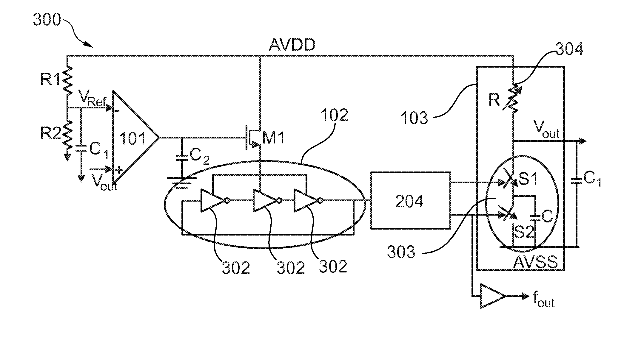
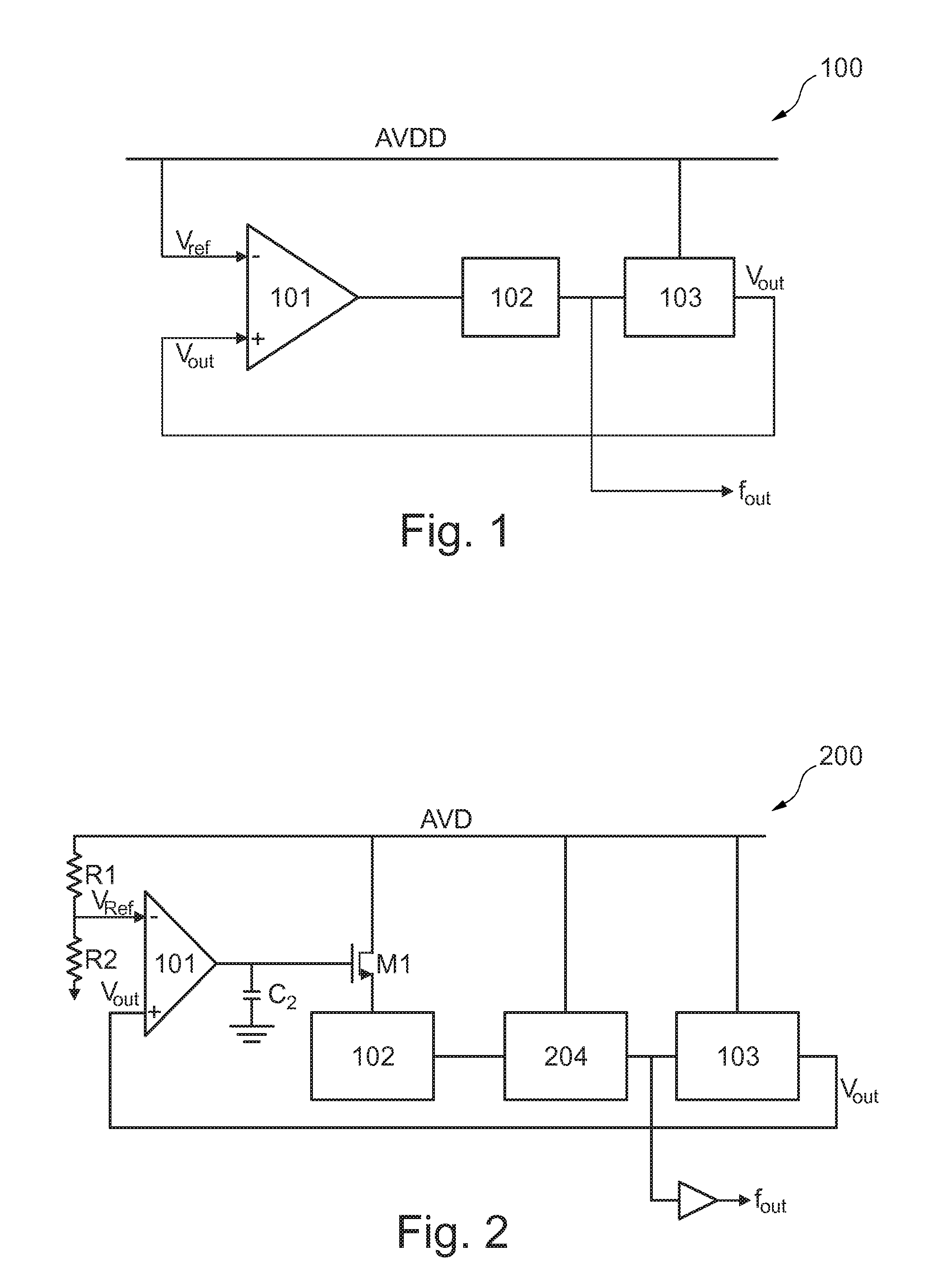
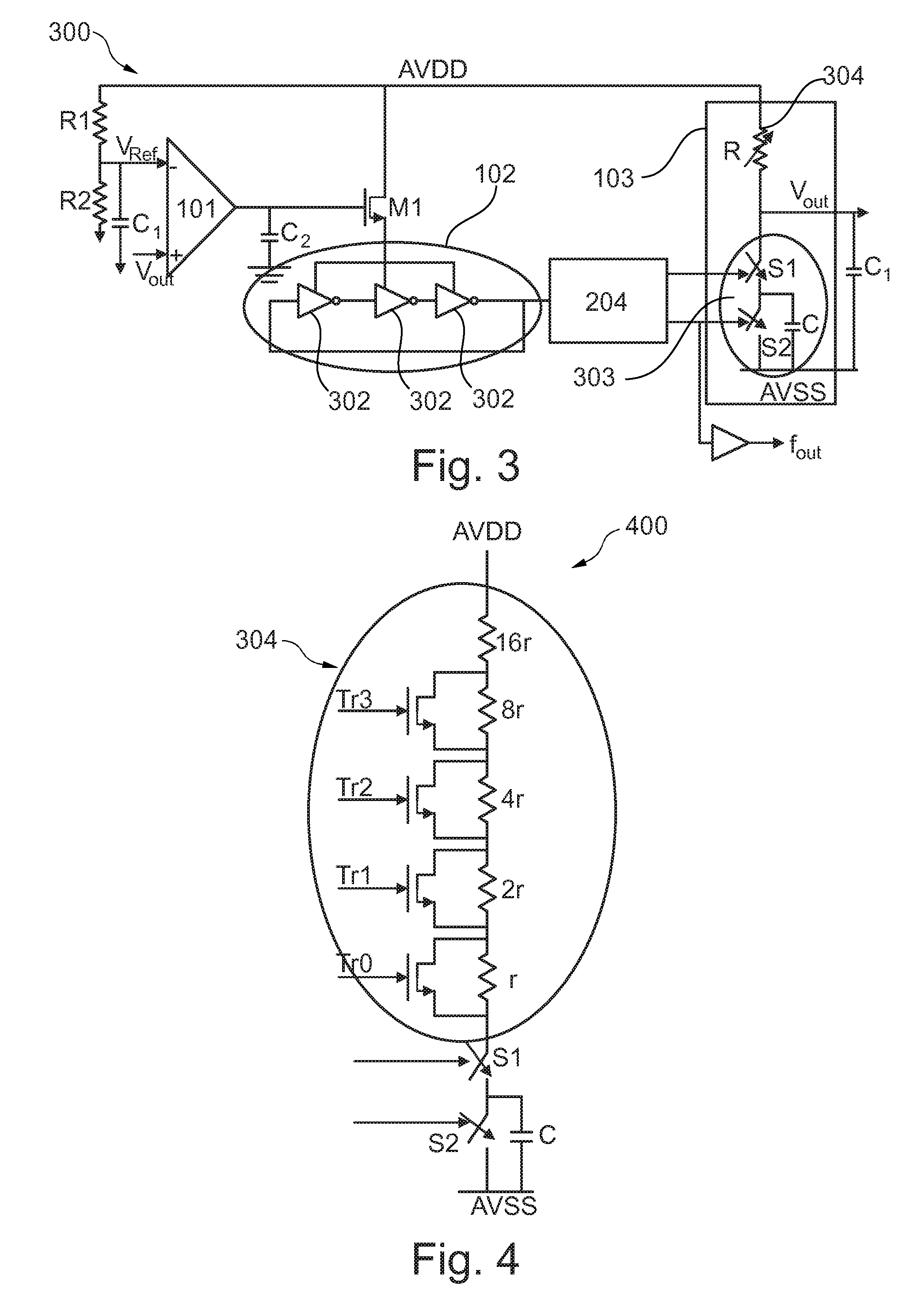
[0053]As shown in FIG. 1, the described oscillator arrangement 100 comprises a current controlled oscillator 102, a frequency to voltage converter 103, and an operational amplifier 101. The oscillator arrangement is connectable to a supply voltage source, being available via the supply line AVD or AVDD.

[0054]The current controlled oscillator 102 is adapted to generate a clock signal fout based on a control voltage signal. The generated clock signal is supplied to the frequency to voltage converter 103. The frequency to voltage converter 103 generates an output voltage signal Vout based on the generated clock signal fout and based on the supply voltage signal.

[0055]The operational amplifier 101 receives the output voltage signal Vout as a feedback signal at a first (here the positive) input terminal and receives a reference voltage si...


PUM


Abstract

There is provided an oscillator arrangement for generating a clock signal. The oscillator arrangement comprises a current controlled oscillator, a frequency to voltage converter, and an operational amplifier. The oscillator arrangement is connectable to a supply voltage source. In one embodiment, the oscillator arrangement may achieve a stable clock frequency insensitive to supply and temperature variation with low current consumption and low area. This may be achieved by using Vref and Vout as input signals to the operational amplifier, both signals being directly derived from the supply voltage. In a further embodiment, a trimming resistor may be used in the frequency to voltage converter for adjusting the frequency.

Description

CROSS-REFERENCE TO THE RELATED APPLICATIONS[0001]This application claims the priority under 35 U.S.C. §119 of European patent application no. 12174201.9, filed on Jun. 28, 2012, the contents of which are incorporated by reference herein.FIELD OF THE INVENTION[0002]The invention relates to an oscillator arrangement for generating a clock signal.[0003]Further, the invention relates to a semiconductor device comprising the oscillator arrangement.[0004]Beyond this, the invention relates to a method of generating a clock signal.[0005]Moreover, the invention relates to a computer-readable medium.[0006]Furthermore, the invention relates to a program element.BACKGROUND OF THE INVENTION[0007]In semiconductor devices, for instance Systems on a Chip (SoC), a clock signal typically needs to be generated for many applications and functions. Conventionally, phase locked loop (PLL's) are used for clock generation in bigger SoCs as they faithfully multiply a reference crystal clock to a stable high...

Claims


Application Information

Patent Timeline
Patent Type & Authority Patents(United States)
IPC IPC(8): H03L7/099H03L1/00H03L7/02
CPCH03L1/00H03L7/02
Inventor PATASANI, MANOJ KUMARTRIVEDI, RONAK PRAKASHCHANDRA
Owner NXP BV
Why Eureka
Try Eureka