Chuck and semiconductor process using the same

a semiconductor and chuck technology, applied in the direction of semiconductor/solid-state device testing/measurement, photomechanical equipment, instruments, etc., can solve the problems of poor uniformity of the films subsequently formed on the wafer, warpage of the wafer, so as to improve the uniformity of the material layer formed on the semiconductor substrate, reduce the risk of warpage, and reduce the effect of chuck and semiconductor process

Active Publication Date: 2015-05-05
UNITED MICROELECTRONICS CORP
View PDF3 Cites 7 Cited by
  • Summary
  • Abstract
  • Description
  • Claims
  • Application Information

AI Technical Summary

Benefits of technology

[0021]In accordance with the aforementioned apparatus of the semiconductor process, the chuck has a plurality of holes for holding the semiconductor substrate, and the vacuum source is used for providing vacuum suction through the holes to make the semiconductor substrate be subjected to varied suction intensities according to the warpage level thereof, so that the warpage of the semiconductor substrate can be eliminated. Therefore, the yield of the process of the semiconductor substrate performed as the semiconductor substrate placed on the chuck can be increased and the uniformity of the material layer formed on the semiconductor substrate may be improved.

Problems solved by technology

It is currently common to form a plurality of films on a wafer in a semiconductor process, so the wafer is subject to warpage because of the pressure or stress resulting from the films stacked thereon.
On the contrary, the warping wafer would result in poor uniformity of the films subsequently formed on the wafer.
Therefore, it is an important issue to reduce the degree of warpage of the wafer.

Method used


Image

  • Chuck and semiconductor process using the same
  • Chuck and semiconductor process using the same
  • Chuck and semiconductor process using the same

Examples


Embodiment Construction

[0030]The present invention will now be described more specifically with reference to the following embodiments. It is to be noted that the following descriptions of preferred embodiments of this invention are presented herein for purpose of illustration and description only. It is not intended to be exhaustive or to be limited to the precise form disclosed.

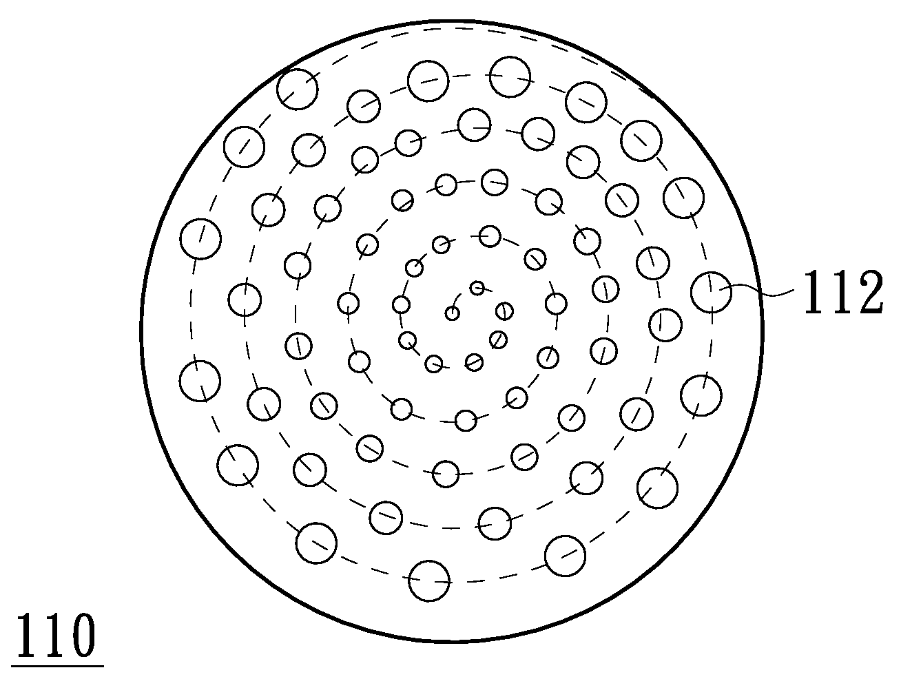
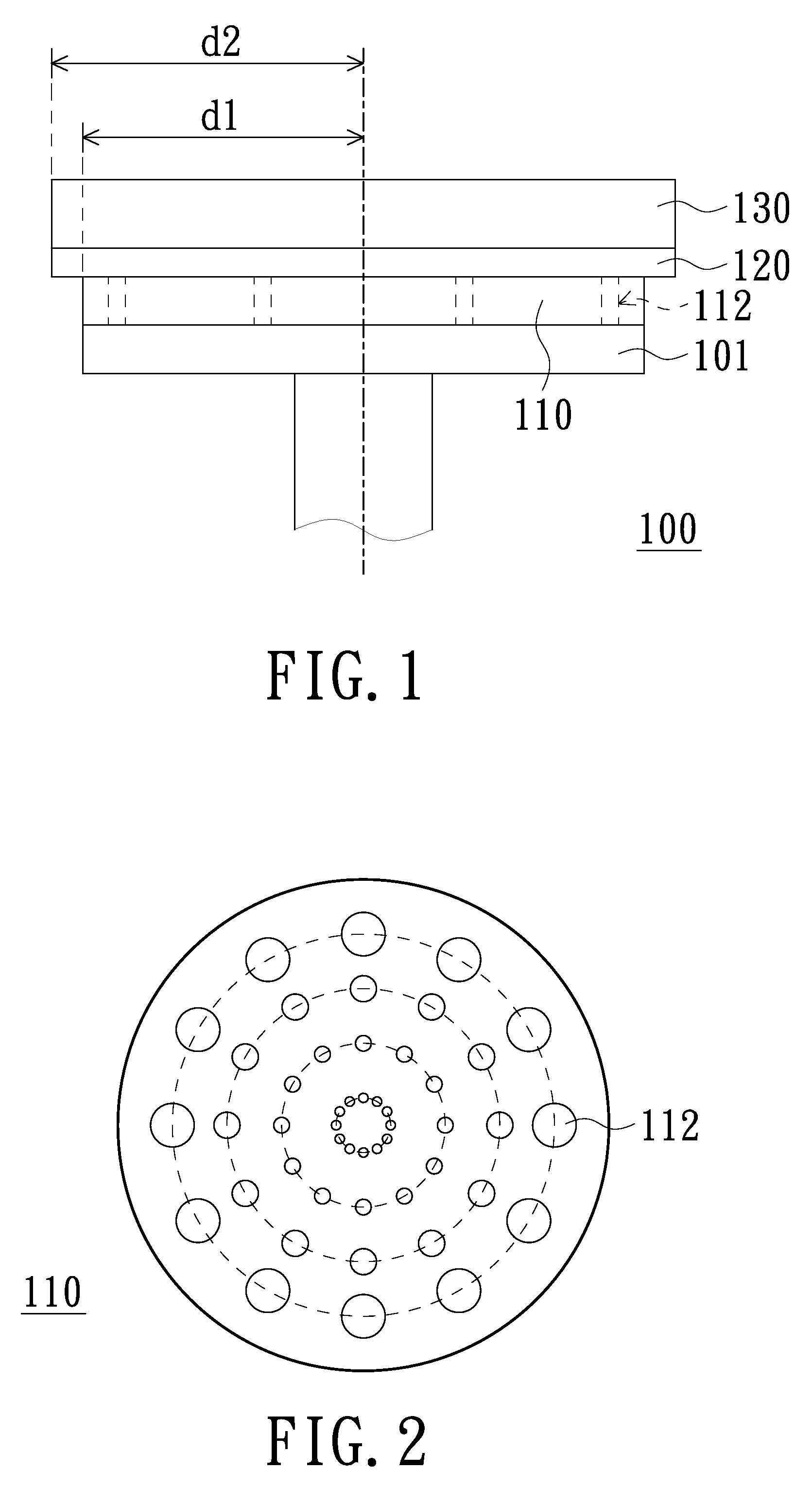
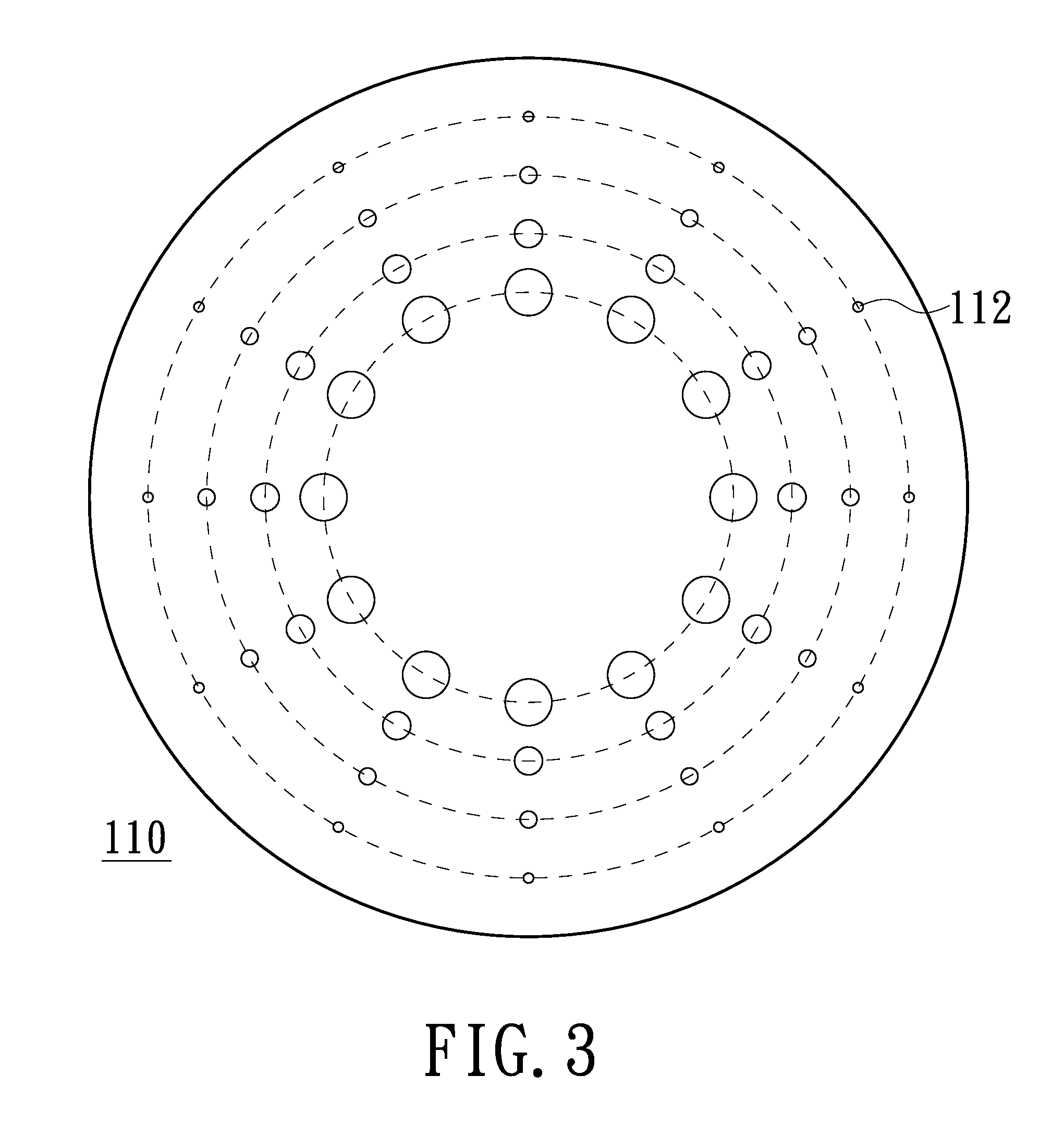
[0031]FIG. 1 is a cross-sectional schematic view illustrating an apparatus of semiconductor process 100 in accordance with an embodiment of the invention. Referring to FIG. 1, the apparatus of semiconductor process 100 includes a chuck 110, which has a plurality of holes 112, and at least one vacuum source 101. For operation, a semiconductor substrate 120, such as a wafer, is placed and held on the chuck 110 by vacuum suction provided from the vacuum source 101 through the holes 112. In detail, the semiconductor substrate 120 can be subjected to varied suction intensities.

[0032]In this embodiment, the sizes of the holes 112, e.g....


PUM

PropertyMeasurementUnit
radius d1aaaaaaaaaa
semiconductoraaaaaaaaaa
sizesaaaaaaaaaa

Abstract

An apparatus of semiconductor process including a chuck and a vacuum source is provided. The chuck has a plurality of holes for holding a semiconductor substrate, and the vacuum source is used for providing vacuum suction through the holes to make the semiconductor substrate be subjected to varied suction intensities according to a warpage level thereof.

Description

BACKGROUND[0001]1. Technical Field[0002]The present invention relates generally to semiconductor apparatus and process, and more particularly, to a chuck and a semiconductor process using the same.[0003]2. Description of the Related Art[0004]It is currently common to form a plurality of films on a wafer in a semiconductor process, so the wafer is subject to warpage because of the pressure or stress resulting from the films stacked thereon. On the contrary, the warping wafer would result in poor uniformity of the films subsequently formed on the wafer. Therefore, it is an important issue to reduce the degree of warpage of the wafer.BRIEF SUMMARY[0005]In accordance with one aspect of the present invention, an apparatus of semiconductor process including a chuck and a vacuum source is provided. The chuck has a plurality of holes for holding a semiconductor substrate and the vacuum source is used for providing vacuum suction through the holes to make the semiconductor substrate be subje...

Claims


Application Information

Patent Timeline
Patent Type & Authority Patents(United States)
IPC IPC(8): H01L21/683
CPCH01L21/6838G03F7/707G03F7/70783Y10T279/11Y10T29/49764G03F7/20H01L22/12H01L22/20H01L21/6836
Inventor JANG, CHUNG-SUNGLIN, MING-TSELIN, YUNG-CHANG
Owner UNITED MICROELECTRONICS CORP
Why Eureka
Try Eureka