Display panel and method of manufacturing the same

a technology of display panel and manufacturing method, which is applied in the field of display panel, can solve the problems of relative high manufacturing cost, and achieve the effect of maintaining the aperture ratio of the display panel and reducing the number of poor performing pixels

Inactive Publication Date: 2015-05-12
SAMSUNG DISPLAY CO LTD
View PDF14 Cites 1 Cited by
  • Summary
  • Abstract
  • Description
  • Claims
  • Application Information

AI Technical Summary

Benefits of technology

[0030]In accordance with one or more exemplary embodiment of the invention, a display panel and a method of manufacturing the same include the black matrix overlapped with the gate lines, and the hole in the black matrix exposes the color filter layer, so that an aperture ratio of the display panel may be maintained and poor performing pixels may be decreased.

Problems solved by technology

The array substrate includes a first base substrate and the color filter substrate includes a second base substrate, thus resulting in a relatively high manufacturing cost since the display panel includes two base substrates.

Method used


Image

  • Display panel and method of manufacturing the same
  • Display panel and method of manufacturing the same
  • Display panel and method of manufacturing the same

Examples


Embodiment Construction

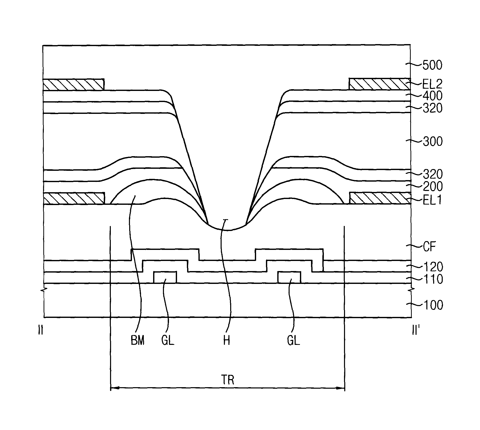
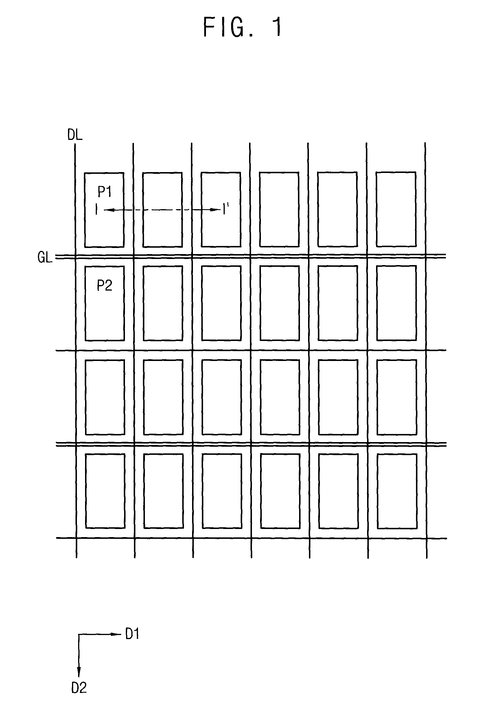
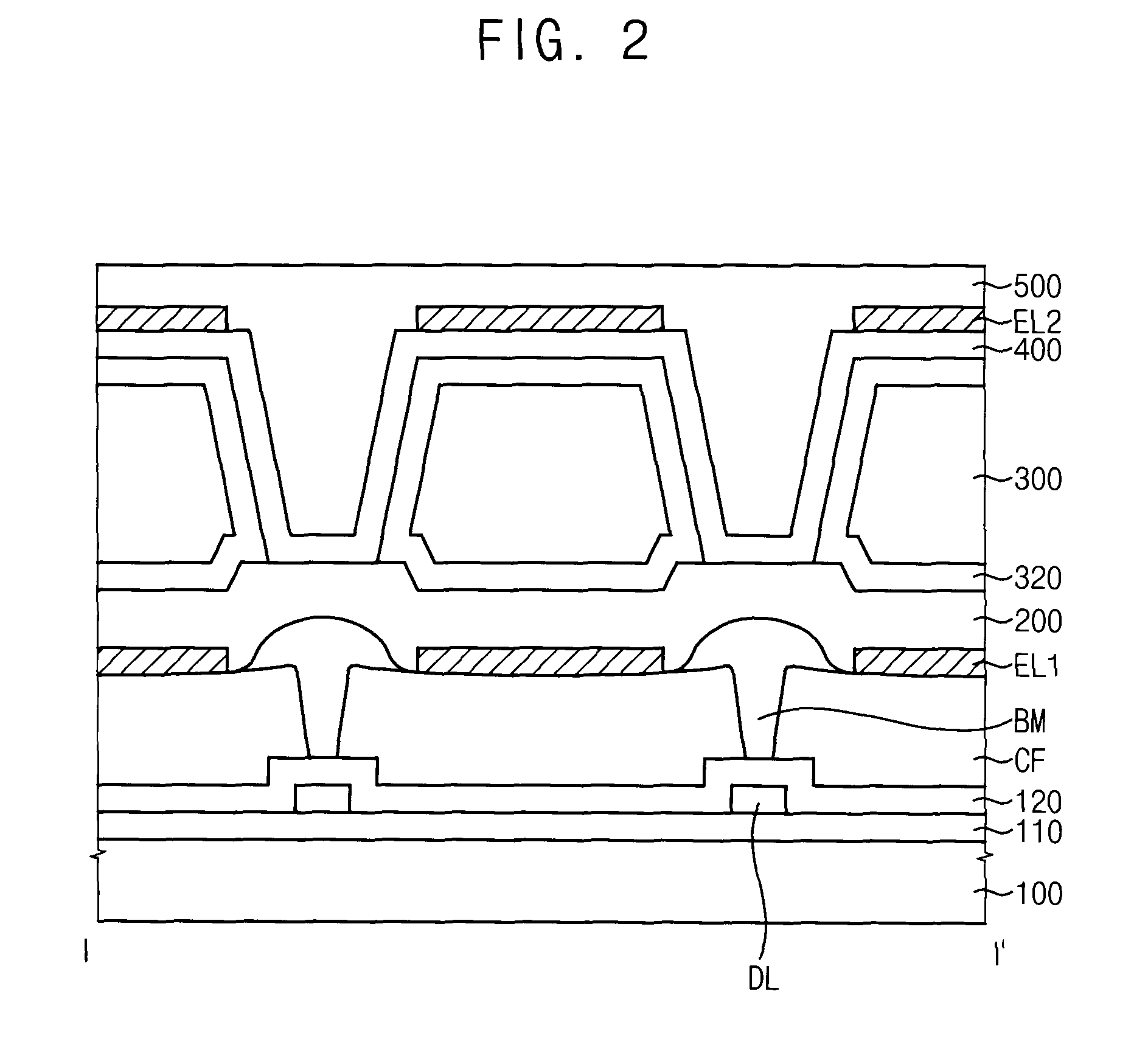
[0037]It will be understood that when an element or layer is referred to as being “on” or “connected to” another element or layer, the element or layer can be directly on or connected to another element or layer or intervening elements or layers. In contrast, when an element is referred to as being “directly on” or “directly connected to” another element or layer, there are no intervening elements or layers present. As used herein, connected may refer to elements being physically and / or electrically connected to each other. In the drawings, the size and relative sizes of layers and regions may be exaggerated for clarity.

[0038]It will be understood that, although the terms first, second, third, etc., may be used herein to describe various elements, components, regions, layers and / or sections, these elements, components, regions, layers and / or sections should not be limited by these terms. These terms are only used to distinguish one element, component, region, layer or section from a...


PUM

PropertyMeasurementUnit
lengthaaaaaaaaaa
widthaaaaaaaaaa
widthaaaaaaaaaa

Abstract

A display panel includes a substrate including a plurality of thin-film transistors thereon, a plurality of gate lines respectively connected to a thin film transistor and disposed on the substrate, a color filter layer disposed on the substrate and the gate lines, a black matrix disposed on the color filter and overlapped with the gate lines, and a hole defined in the black matrix and exposing the color filter layer, a first electrode disposed on the color filter and electrically connected to the thin-film transistor and an image displaying layer disposed on the first electrode.

Description

[0001]This application claims priority to Korean Patent Application No. 10-2013-0068194, filed on Jun. 14, 2013, and all the benefits accruing therefrom under 35 U.S.C. §119, the disclosure of which is incorporated by reference herein in its entirety.BACKGROUND[0002](1) Field[0003]Exemplary embodiments of the invention relate to a display panel and a method of manufacturing the same, and more particularly, to a display panel including one base substrate and a method of manufacturing the same.[0004](2) Description of the Related Art[0005]A display panel includes an array substrate, a color filter substrate, and a liquid crystal layer disposed between the array substrate and the color filter substrate. The array substrate includes switching elements, and the color filter substrate includes color filters disposed therein. The array substrate includes a first base substrate and the color filter substrate includes a second base substrate, thus resulting in a relatively high manufacturing...

Claims


Application Information

Patent Timeline
Patent Type & Authority Patents(United States)
IPC IPC(8): G02F1/136G02F1/1335G02F1/1333
CPCG02F1/133514G02F1/133512G02F1/133528G02F1/133377G02F1/136209G02F2001/136222G02F1/136222H01L27/1225H01L29/42384H01L29/4908H01L29/51H01L29/66742H01L29/66969H01L29/7869
Inventor CHAE, SEUNG-YEONCHOI, SANG-GUNLEE, A-RAMCHA, TAE-WOON
Owner SAMSUNG DISPLAY CO LTD
Why Eureka
Try Eureka