Method and apparatus for the formation of dielectric layers

a dielectric layer and dielectric film technology, applied in the field of dielectric formation, can solve the problems of poor electrical performance, high leakage current, and preventing the use of high temperature processing

Inactive Publication Date: 2002-01-24
APPLIED MATERIALS INC
View PDF2 Cites 283 Cited by
  • Summary
  • Abstract
  • Description
  • Claims
  • Application Information

AI Technical Summary

Benefits of technology

[0024] In one embodiment of the present invention remotely generated active atomic species are used to passivate a silicon substrate prior to the formation of a gate dielectric layer or are used to passivate a capacitor electrode prior to the formation of a capacitor dielectric layer thereon. It is to be appreciated that as gate and capacitor dielectric film thicknesses shrink, to enable the fabrication of high density integrated circuits, the atomic level interfaces between the substrate and dielectric are becoming increasingly more important for device reliability and performance. By passivating a substrate with remotely generated active atomic species one can improve the atomic level interfaces between the substrate and the dielectric film and thereby improve device reliability and performance.
[0025] In another embodiment of the present invention, remotely generated active atomic species are used to anneal an active dielectric film, such as a gate dielectric or a capacitor dielectric. According to this embodiment of the present invention a dielectric film is deposited over substrate. The dielectric film is then exposed to remotely generated active atomic species, such as reactive oxygen atoms or reactive nitrogen atoms. The highly energized atomic species readily react with the dielectric film to fill vacancies in the lattice which left unfilled can lead to high leakage currents and poor device performance. The remotely generated active atomic species can be used to anneal a wide range of dielectrics such as but not limited to silicon oxides, such as silicon dioxide and silicon oxynitride, transition-metal dielectrics such as tantalum pentaoxide (Ta.sub.2O.sub.5), titanium oxide (TiO.sub.2) and titanium doped tanatalum pentaoxide, as well as ferroelectric and piezoelectric dielectrics such as BST, and PZT. Additionally, active atomic species, such as reactive nitrogen atoms can be used to anneal dielectric barrier layers, such as silicon nitride, to improve their barrier qualities.
[0026] In an embodiment of the present invention the remotely generated active atomic species are provided into the deposition chamber while the dielectric film is being deposited. In this way the dielectric film is annealed as it is deposited thereby eliminating the need for a separate anneal step.
[0027] As such remotely generated active atomic species can be used in all phases of dielectric film formation including substrate passivation prior to dielectric layer deposition, annealing during dielectric deposition and annealing after dielectric deposition. In this way high quality, high performance capacitor and gate dielectrics as well as barrier layers can be fabricated.
[0028] In one specific embodiment of the present invention, remotely generated reactive oxygen atoms are used to anneal a transition-metal dielectric used as a capacitor dielectric in a dynamic random access memory (DRAM). In this embodiment of the present invention a transition-metal dielectric film is formed by chemical vapor deposition (CVD) over a bottom electrode of a DRAM cell. The transition-metal film is then annealed at a temperature less than 400.degree. C. with reactive oxygen atoms formed in a chamber separate from the anneal chamber. The remotely generated reactive oxygen atoms readily react with the deposited transition-metal film and satisfy open sites in the film. Additionally, the reactive oxygen atoms remove carbon contaminates by chemically reacting with carbon and forming carbon dioxide (CO.sub.2) vapor which is then exhausted from the chamber. By annealing the dielectric film with remotely generated reactive oxygen atoms, the leakage current of the film can be substantially reduced. A top capacitor electrode can then be formed on the high quality high dielectric constant film thereby improving the performance and reliability of the fabricated cell.

Problems solved by technology

A problem with utilizing such high anneal temperatures is that dielectric films such as tantalum pentaoxide crystallize when exposed to high temperatures which can lead to high leakage currents.
Additionally high anneal temperatures can cause other ions to diffuse into the film, especially at the interfaces of the devices, and cause poor electrical performance.
Still further some processes utilize materials with low melting points which preclude subsequent use of high temperature processing.

Method used


Image

  • Method and apparatus for the formation of dielectric layers
  • Method and apparatus for the formation of dielectric layers
  • Method and apparatus for the formation of dielectric layers

Examples


Embodiment Construction

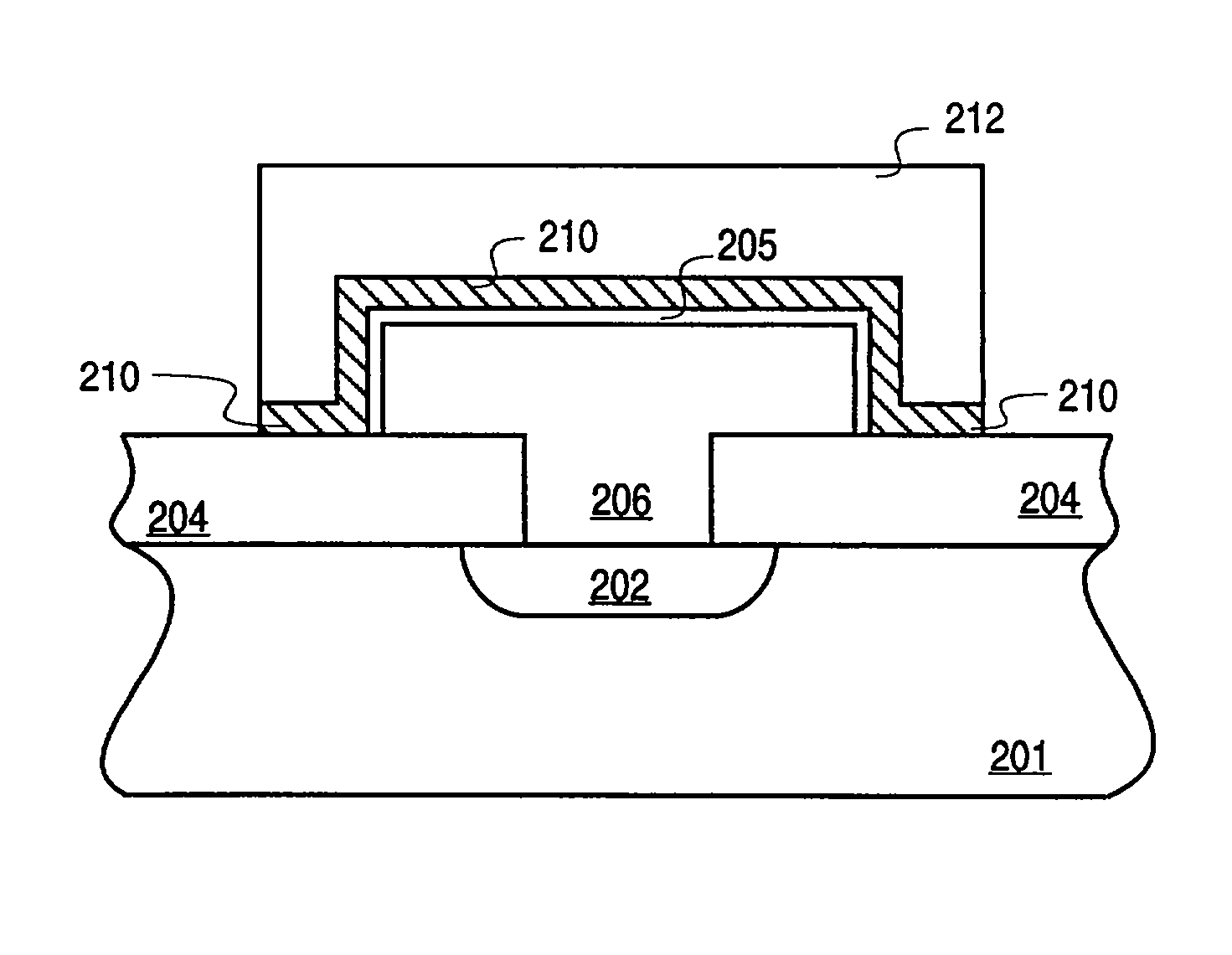
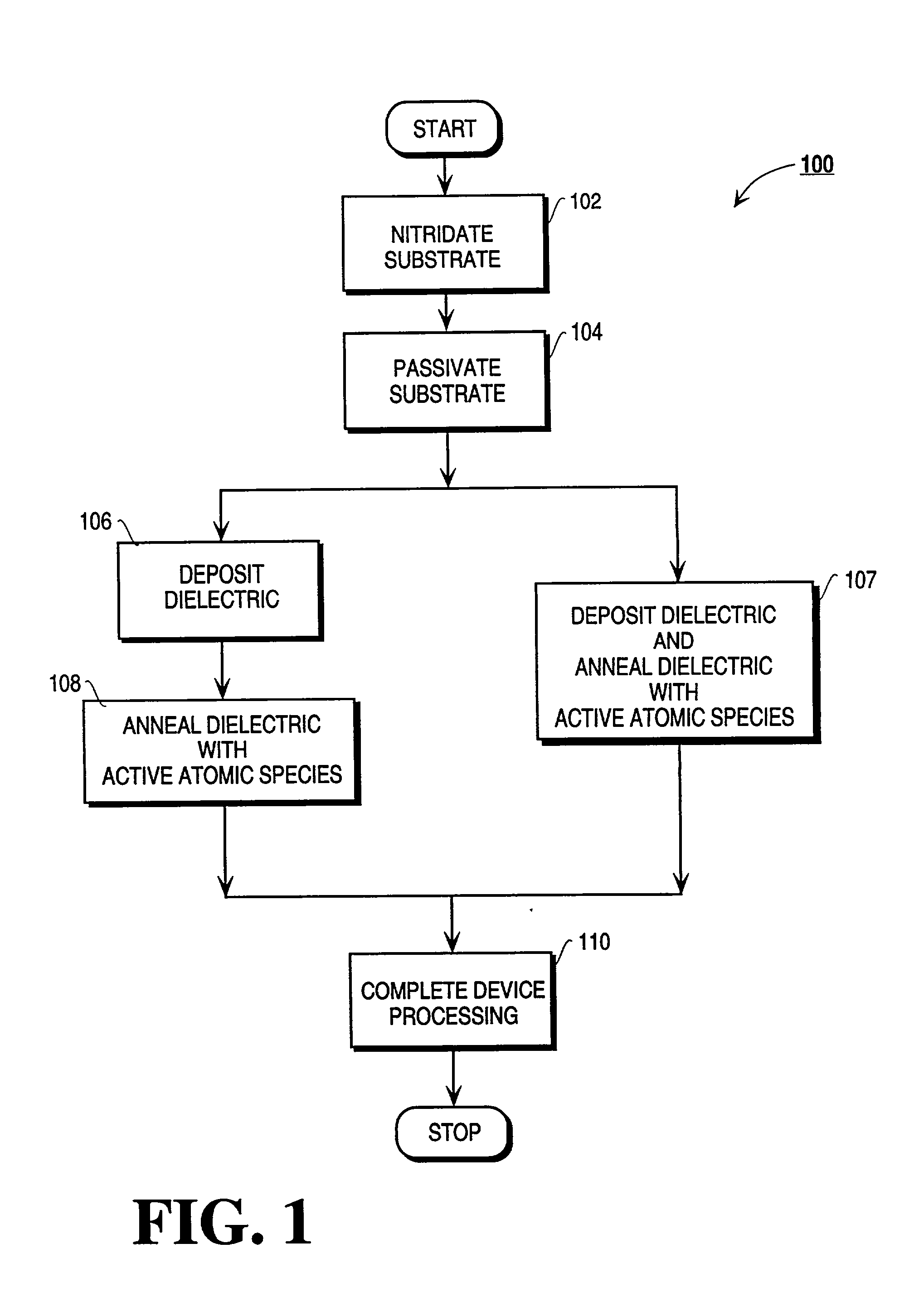
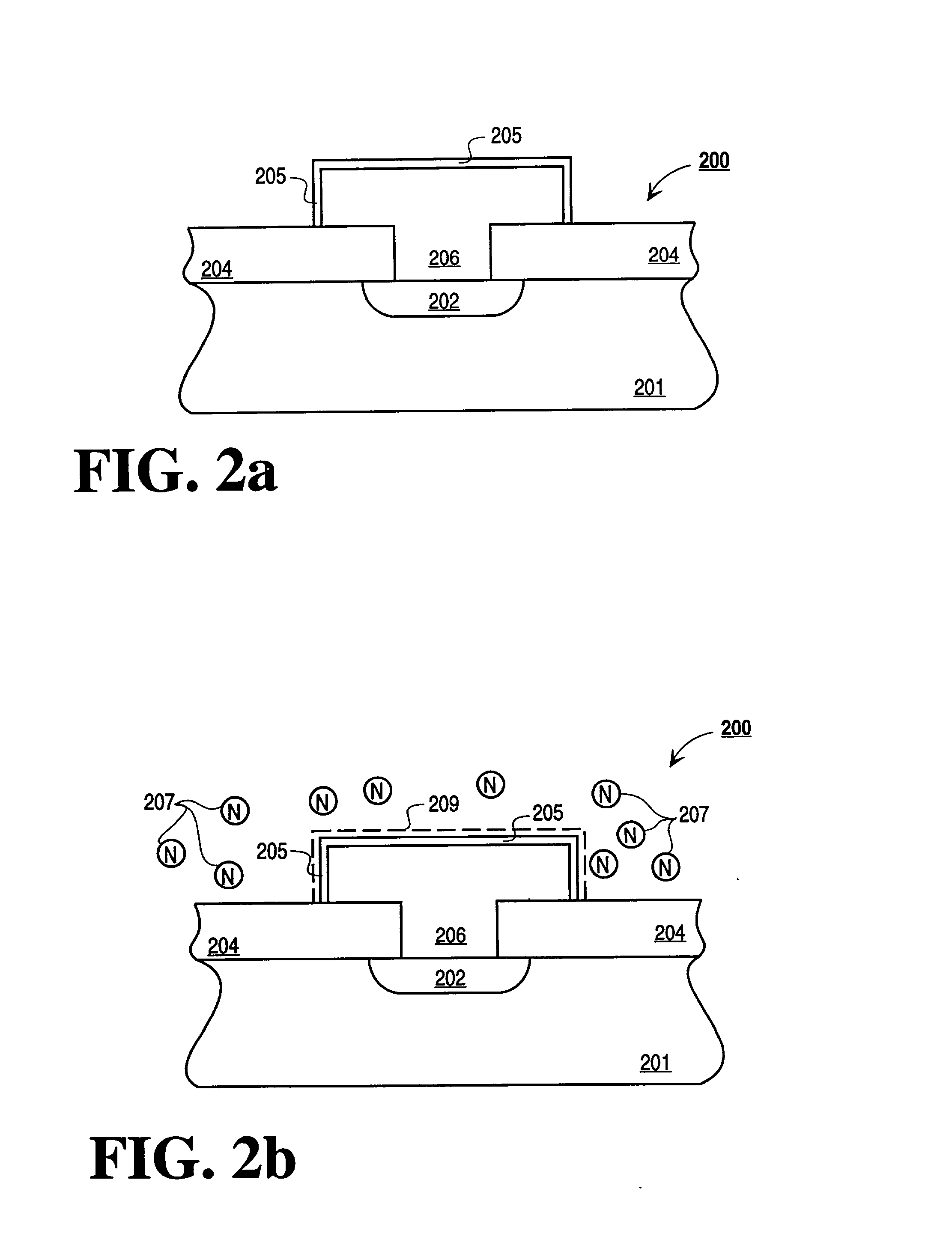
[0022] The present invention describes a novel method and apparatus for annealing a dielectric film. In the following description numerous specific details such as specific equipment configurations, and process parameters are set forth in order to provide a thorough understanding of the present invention. One skilled in the art will appreciate the ability to use alternative configurations and process details to the disclosed specifics without departing from the scope of the present invention. In other instances, well known semiconductor processing equipment and methodology have not been described in detail in order to not unnecessarily obscure the present invention.

[0023] The present invention describes a novel method and apparatus for passivating and / or annealing films. According to the present invention highly reactive atomic species are used to nitridate, passivate, deposit and anneal films. The highly reactive atomic species are formed in a plasma created by exposing an anneal g...


PUM

PropertyMeasurementUnit
temperatureaaaaaaaaaa

Abstract

A method and apparatus for forming and annealing a dielectric layer. According to the present invention an active atomic species is generated in a first chamber. A dielectric layer formed on a substrate is then exposed to the active atomic species in a second chamber, wherein the second chamber is remote from the first chamber.

Description

[0001] 1. Field of the Invention[0002] The present invention relates to the field of dielectric formation and more specifically to a method and apparatus for annealing a dielectric film.[0003] 2. Discussion of Related Art[0004] Integrated circuits are made up of literally millions of active and passive devices such as transistors, capacitors and resistors. In order to provide more computational power and / or more storage capability in an integrated circuit, device features are reduced or scaled down in order to provide higher packing density of devices. An important feature to enable scaling of devices is the ability to form high quality, high dielectric constant films for capacitor and gate dielectrics.[0005] High dielectric constant films are generally ceramic films (i.e., metal-oxides) such as tantalum pentaoxide and titanium oxide. When these films are deposited they tend to have vacancies at the anionic (oxygen) sites in the lattice. Presently these vacancies are filled by annea...

Claims


Application Information

Patent Timeline
Patent Type & Authority Applications(United States)
IPC IPC(8): C23C14/58C23C16/40C23C16/56H01L21/02H01L21/314H01L21/316H01L21/822H01L21/8242H01L27/04H01L27/108
CPCC23C16/56H01L21/31604H01L21/31691H01L28/55C23C14/58C23C16/405H01L21/02315H01L21/02197H01L21/0214H01L21/02164H01L21/02247H01L21/02255H01L21/02329H01L21/02351
Inventor NARWANKAR, PRAVIN K.SAHIN, TURGUTURDAHL, RANDALL S.VELAGA, ANKINEEDULIU, PATRICIA
Owner APPLIED MATERIALS INC
Why Eureka
Try Eureka