Organic light emitting diode display device for sensing pixel current and pixel current sensing method thereof

a light-emitting diode display device and pixel current technology, applied in the field of organic light-emitting diode display devices, can solve the problems of generating residual images, reducing the lifespan of amoled display panels, generating deviations in driving tfts of pixels, etc., to reduce the number of reference lines, increase the pixel aperture ratio, and reduce the number of reference channels

Active Publication Date: 2015-05-19
LG DISPLAY CO LTD
View PDF13 Cites 33 Cited by
  • Summary
  • Abstract
  • Description
  • Claims
  • Application Information

AI Technical Summary

Benefits of technology

[0010]An object of the present invention is to provide an OLED display device for sensing pixel current which is capable of rapidly sensing current of each pixel to compensate for a luminance deviation among pixels and a pixel current sensing method thereof.
[0011]An object of the present invention is to provide an OLED display device for sensing pixel current, which is capable of reducing the scale of a pixel current sensing circuit included therein, and a pixel current sensing method thereof.
[0032]As described above, according to the OLED display device for sensing pixel current and the pixel current sensing method thereof according to the present invention, at least two pixels adjacent to each other in the horizontal direction share a reference line, and at least two pixels sharing each reference line are time-division-driven to sense characteristics of the at least two pixels through the reference line and reference channel shared by the pixels, and thus the number of reference lines and the number of reference channels can be reduced to lower than half the number of data lines. A reduction in the number of reference lines can increase a pixel aperture ratio, compared to a conventional OLED display device in which pixels do not share a reference line. In addition, a reduction in the number of reference channels can decrease the size or number of data driver ICs, compared to the conventional OLED display device in which pixels do not share a reference line.
[0033]Furthermore, the OLED display device for sensing pixel current and the pixel current sensing method thereof according to the present invention can easily sense current of each pixel at a high speed through a data driver. Accordingly, the present invention can sense and compensate for not only an initial characteristic deviation among driving TFTs but also a characteristic deviation due to deterioration of the driving TFTs by inserting a sensing mode between display modes in which the OLED display device is driven and sensing current of each pixel after shipment of products as well as during a test process before shipment of products. Accordingly, the lifespan and picture quality of the OLED display device can be improved.

Problems solved by technology

However, in the OLED display device, pixels may have different driving TFT threshold voltages Vth and mobility due to process variation, causing OLED driving current to be different for respective OLEDs, generating a deviation in characteristics of driving TFTs of the pixels.
In general, an initial driving TFT characteristic difference generates unevenness or a pattern on a screen and a characteristic difference due to deterioration of driving TFTs, which occurs when the driving TFTs drive OLEDs, reduces the lifespan of an AMOLED display panel or generates a residual image.
However, since this technique uses a method of sensing current flowing to a power line (VDD or VSS line) of the panel while turning pixels on, current sensing time increases due to a parasitic capacitor located in parallel with the power line, making high-speed sensing difficult when resolution increases.
Furthermore, although a plurality of current sensing circuits may simultaneously sense currents of a plurality of pixels, this increases circuit scale.
Therefore, while the conventional technology can compensate for an initial characteristic deviation among driving TFTs by measuring the initial characteristic deviation during a test process performed before products are shipped, the conventional technology has difficulty in sensing and compensating for characteristic deviation due to deterioration of the driving TFTs, which occurs when OLEDs have been driven after products are shipped.

Method used


Image

  • Organic light emitting diode display device for sensing pixel current and pixel current sensing method thereof
  • Organic light emitting diode display device for sensing pixel current and pixel current sensing method thereof
  • Organic light emitting diode display device for sensing pixel current and pixel current sensing method thereof

Examples


first embodiment

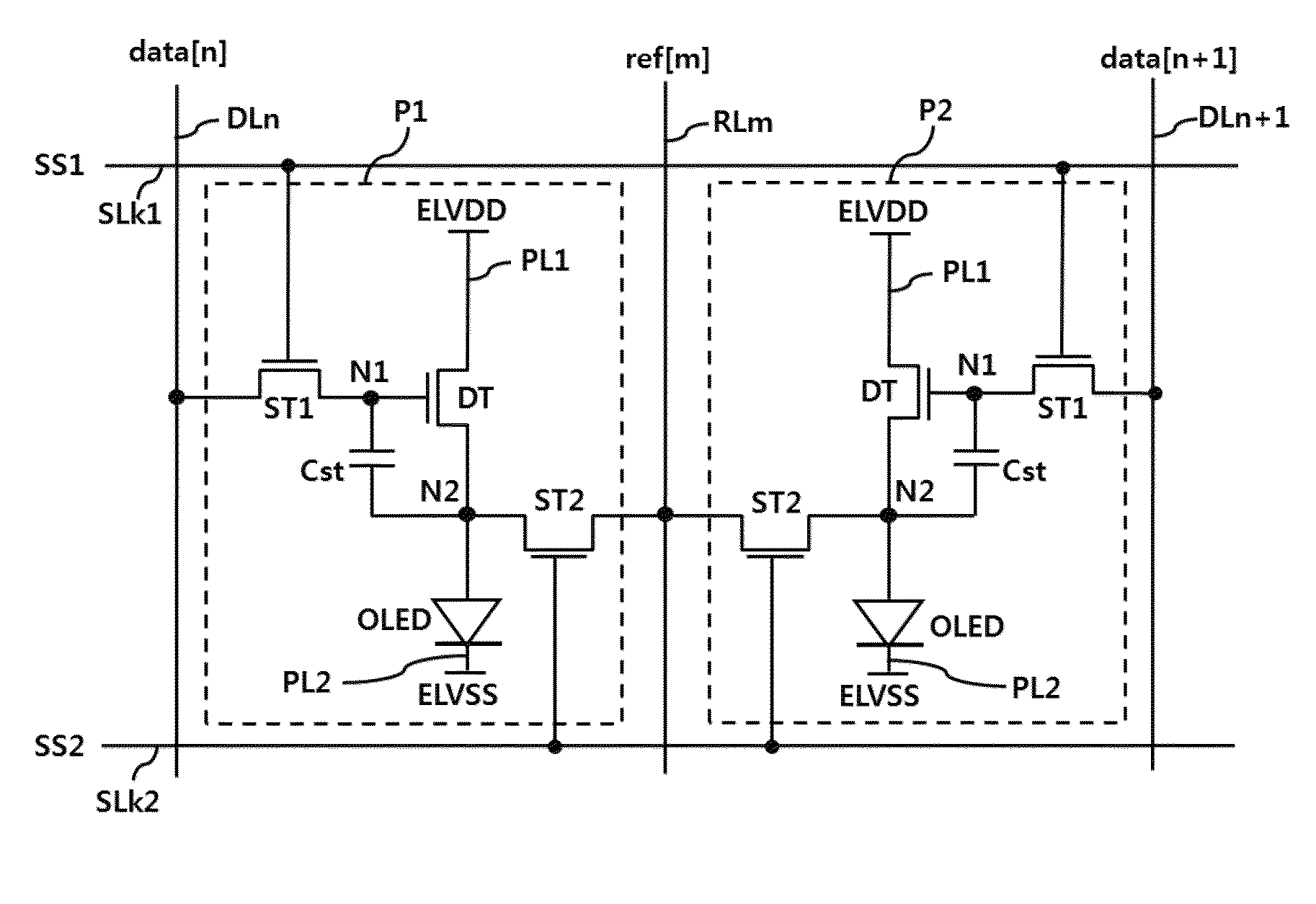
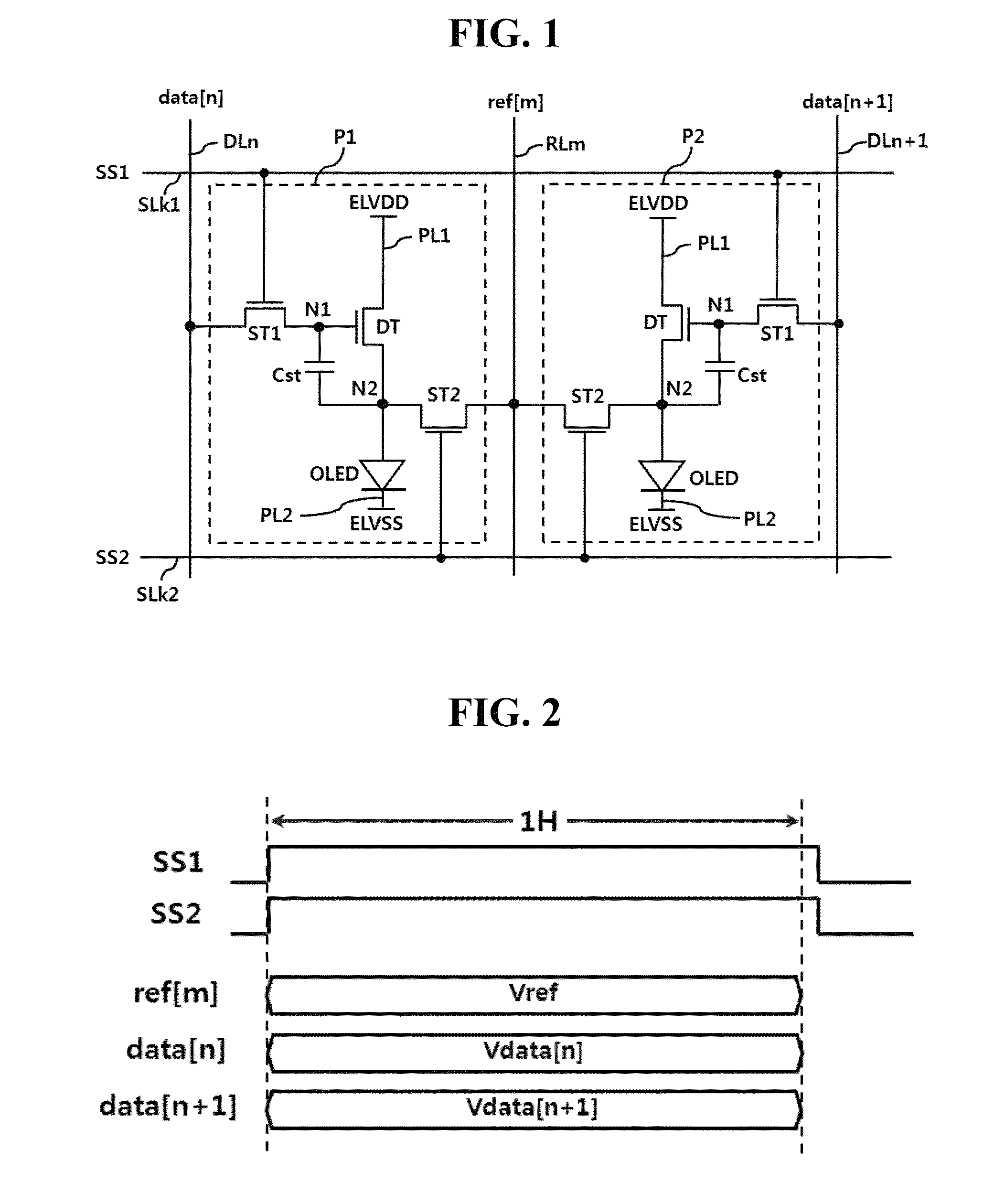
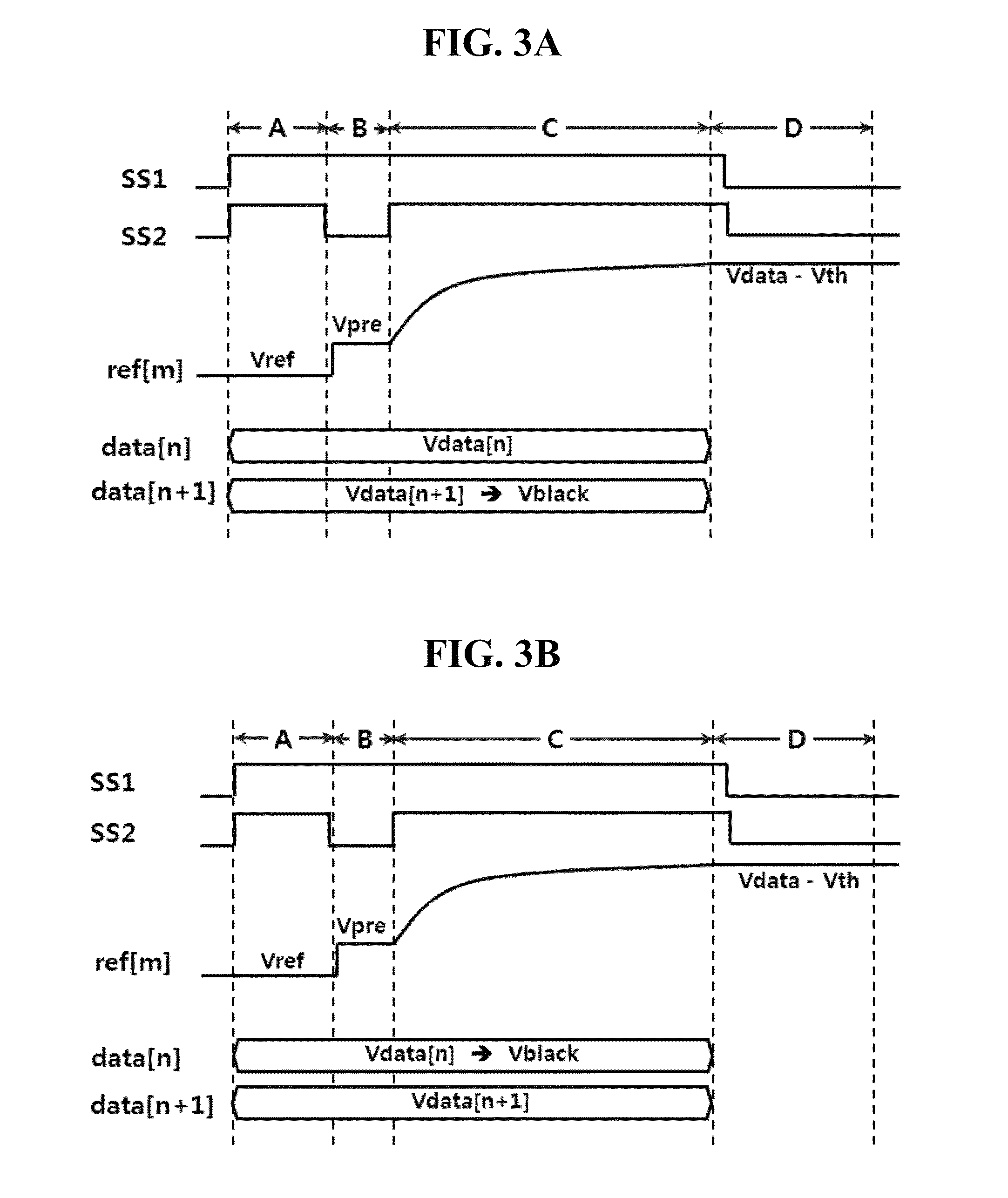
[0048]FIG. 1 is an equivalent circuit diagram of two typical pixels of an OLED display device for sensing pixel current according to the present invention.

[0049]The OLED display device shown in FIG. 1 includes first and second pixels P1 and P2 respectively connected to two neighboring data lines DLn and DLn+1 (n being a natural number), a reference line RLm (m being a natural number) shared by the first and second pixels P1 and P2 between the data lines DLn and DLn+1, and first and second scan lines SLk1 and SLk2 (k being a natural number) that intersect the data lines DLn and DLn+1 and the reference line RLm and are shared by the first and second pixels P1 and P2.

[0050]The first and second pixels P1 and P2 arranged in the horizontal direction respectively represent first and second pixel strings that share the reference line RLm. The first and second pixels P1 and P2 are respectively connected to the two data lines DLn and DLn+1 extended in the vertical direction. The reference lin...

second embodiment

[0089]FIG. 5 is an equivalent circuit diagram of four typical pixels of an OLED display device for sensing pixel current according to the present invention.

[0090]The second embodiment shown in FIG. 5 has the same concept as the first embodiment shown in FIG. 1 and is distinguished from the first embodiment in that each reference line RLm is branched to at least two lines such that four neighboring pixels P1 to P4 in the horizontal direction share one reference line RLm. Accordingly, explanation of components equal to the corresponding components shown in FIG. 1 is omitted or simplified.

[0091]In FIG. 5, first to fourth pixels P1 to P4 arranged in the horizontal direction respectively represent pixel strings. The first to fourth pixels P1 to P4 are respectively connected to four data lines DLn to DLn+3 extended in the vertical direction and commonly connected to first and second scan lines SLk1 and SLk2 extended in the horizontal direction. The reference line RLm is branched to a firs...

third embodiment

[0115]FIG. 9 is an equivalent circuit diagram of two typical pixels of an OLED display device for sensing pixel current according to the present invention.

[0116]The third embodiment shown in FIG. 9 has the same concept as the first embodiment shown in FIG. 1 and is distinguished from the first embodiment in that the second switching TFTs ST2 of the first and second pixels P1 and P2 are respectively connected to the second and third scan lines SLk2 and SLk3. Accordingly, explanation of components equal to the corresponding components shown in FIG. 1 is omitted or simplified.

[0117]Referring to FIG. 9, the first switching TFTs ST1 of the first and second pixels P1 and P2 are commonly connected to the first scan line SLk1, the second switching TFT ST2 of the first pixel P1 is connected to the second scan line SLk2, and the second switching TFT ST2 of the second pixel P2 is connected to the third scan line SLk2. Accordingly, the second switching TFT ST2 of the first pixel P1 can be drive...


PUM


Abstract

The present invention relates to an organic light emitting diode display device capable of sensing driving current of each pixel with a simple configuration to compensate for a luminance deviation between pixels and a pixel current sensing method thereof. The organic light emitting diode display device includes a display panel including 2N (N being a natural number) pixels that share a reference line though which a reference signal is supplied and are respectively connected to 2N data lines through which data signals are applied, and a data driver for driving the 2N pixels sharing the reference line in a time division manner through the data lines, sensing currents of the time-division-driven 2N pixels as voltages through the shared reference line and outputting the sensed currents, in a sensing mode.

Description

[0001]This application claims the benefit of Korean Patent Application No. 10-2012-0078520, filed on Jul. 19, 2012, which is hereby incorporated by reference as if fully set forth herein.BACKGROUND OF THE INVENTION[0002]1. Field of the Invention[0003]The present invention relates to an organic light emitting diode display device, and more particularly, to an organic light emitting diode display device capable of sensing driving current of each pixel with a simple configuration to compensate for a luminance deviation between pixels and a pixel current sensing method thereof.[0004]2. Discussion of the Related Art[0005]An organic light emitting diode (OLED) display device is a self-emission element that makes an organic emission layer emit light according to recombination of electrons and holes. The OLED display device is expected to be a next-generation display device since it is ultra-thin and has high brightness and low driving voltage.[0006]Each pixel constituting the OLED display ...

Claims


Application Information

Patent Timeline
Patent Type & Authority Patents(United States)
IPC IPC(8): G09G5/10G09G3/32G06F3/038G09G3/00
CPCG09G3/3233G09G3/3283G09G5/10G09G3/006G09G2310/0251G09G2320/043G09G2330/12G09G3/3291G09G3/3225G09G2300/043G09G2300/0465G09G2320/0233G09G3/30
Inventor LEE, JI-EUNKIM, BUM-SIKKIM, SEUNG-TAEHA, WON-KYUOH, KIL-HWAN
Owner LG DISPLAY CO LTD
Why Eureka
Try Eureka