Electrically bonded arrays of transfer printed active components

a technology of active components and bonded arrays, which is applied in the direction of laminating printed circuit boards, radiation controlled devices, and semiconductor/solid-state device details. it can solve the problems of poor electronic characteristics of coatings, poor performance of resulting layers, and significant limitations of traditional techniques, so as to reduce the cost of materials and manufacturing equipment, the effect of fewer processing steps

Active Publication Date: 2015-06-02
X DISPLAY CO TECH LTD
View PDF14 Cites 47 Cited by
  • Summary
  • Abstract
  • Description
  • Claims
  • Application Information

AI Technical Summary

Benefits of technology

[0066]Embodiments of the present invention provide high-performance active components over large substrates at a reduced cost in materials and manufacturing equipment, with fewer processing steps and material layers.

Problems solved by technology

However, such coatings typically have relatively poor electronic characteristics.
These methods typically improve the electron mobility of the semiconductor, but the performance of the resulting layer may still be worse than is often desirable.
These traditional techniques have some significant limitations.
Despite processing methods used to improve the performance of thin-film transistors, such transistors have a performance lower than the performance of traditional integrated circuits formed in mono-crystalline semiconductor material.
Semiconductor material and active components can be desired only on portions of the substrate, leading to wasted material and increased material and processing costs.
For example, plastic substrates have a relatively limited chemical and heat tolerance and do not typically survive photo-lithographic processing.
Furthermore, the manufacturing equipment needed to process large substrates with thin-film circuitry is relatively expensive.
While this approach can provide substrates with similar performance as integrated circuits, the size of such substrates is typically limited, for example, to a 12-inch diameter circle, and the wafers are relatively expensive compared to other substrate materials such as glass or polymer.
However, the bonding technique can be expensive, and the processing equipment for the substrates to form the thin-film active components on large substrates remains relatively expensive.
However, these integrated circuits are relatively large and additional layers may not be easily formed over the integrated circuits.
However this method requires etching a significant quantity of material and risks damaging the exposed TFT array.
Moreover, the laser beam that irradiates the object is typically shaped to match the shape of the object, and the laser abrasion can damage the object to be transferred.
Furthermore, the adhesive cure takes time, which can reduce the throughput of the manufacturing system.
This method, however, requires the construction of conductive metal traces over both the integrated circuits and substrate.
Because the integrated circuits have a relatively large relief profile, for example 10 microns, forming such connections can be difficult.
Furthermore, forming the conductive metal traces after the integrated circuits are adhered to the substrates typically subjects the integrated circuits and substrate to photo-lithographic processing steps and can require additional layers of material.

Method used


Image

  • Electrically bonded arrays of transfer printed active components
  • Electrically bonded arrays of transfer printed active components
  • Electrically bonded arrays of transfer printed active components

Examples


Embodiment Construction

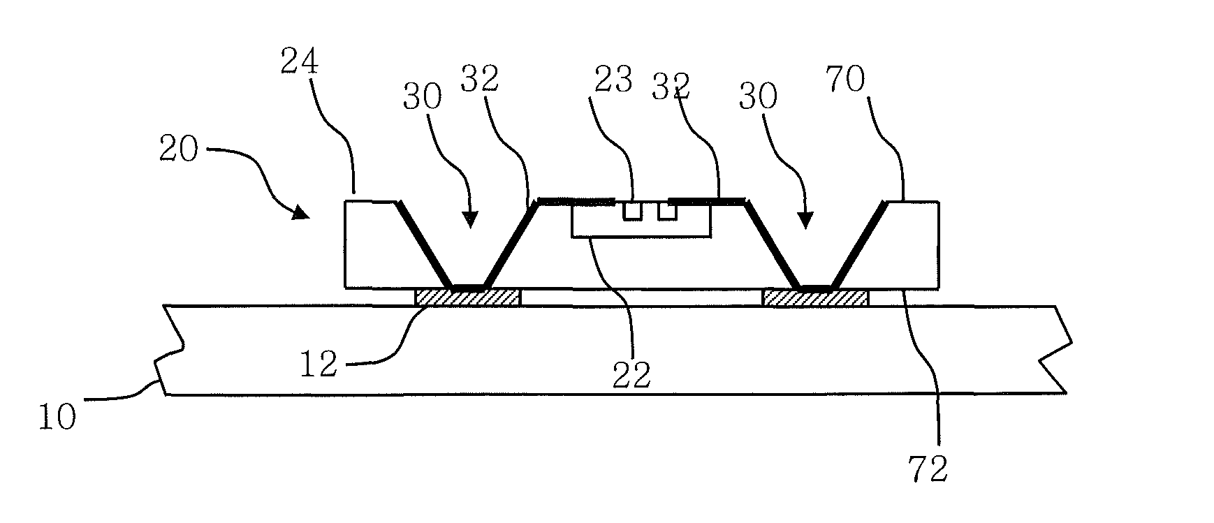
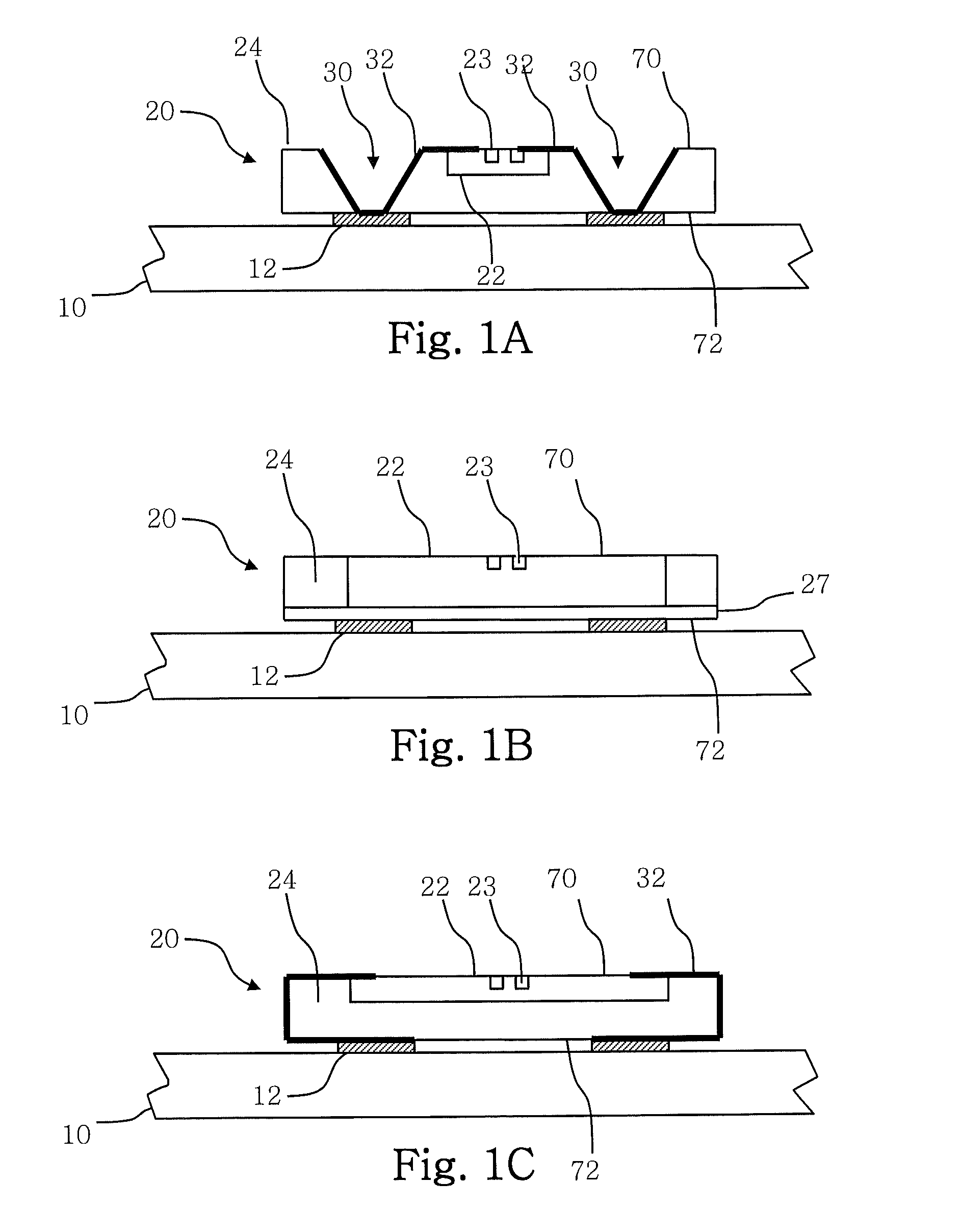
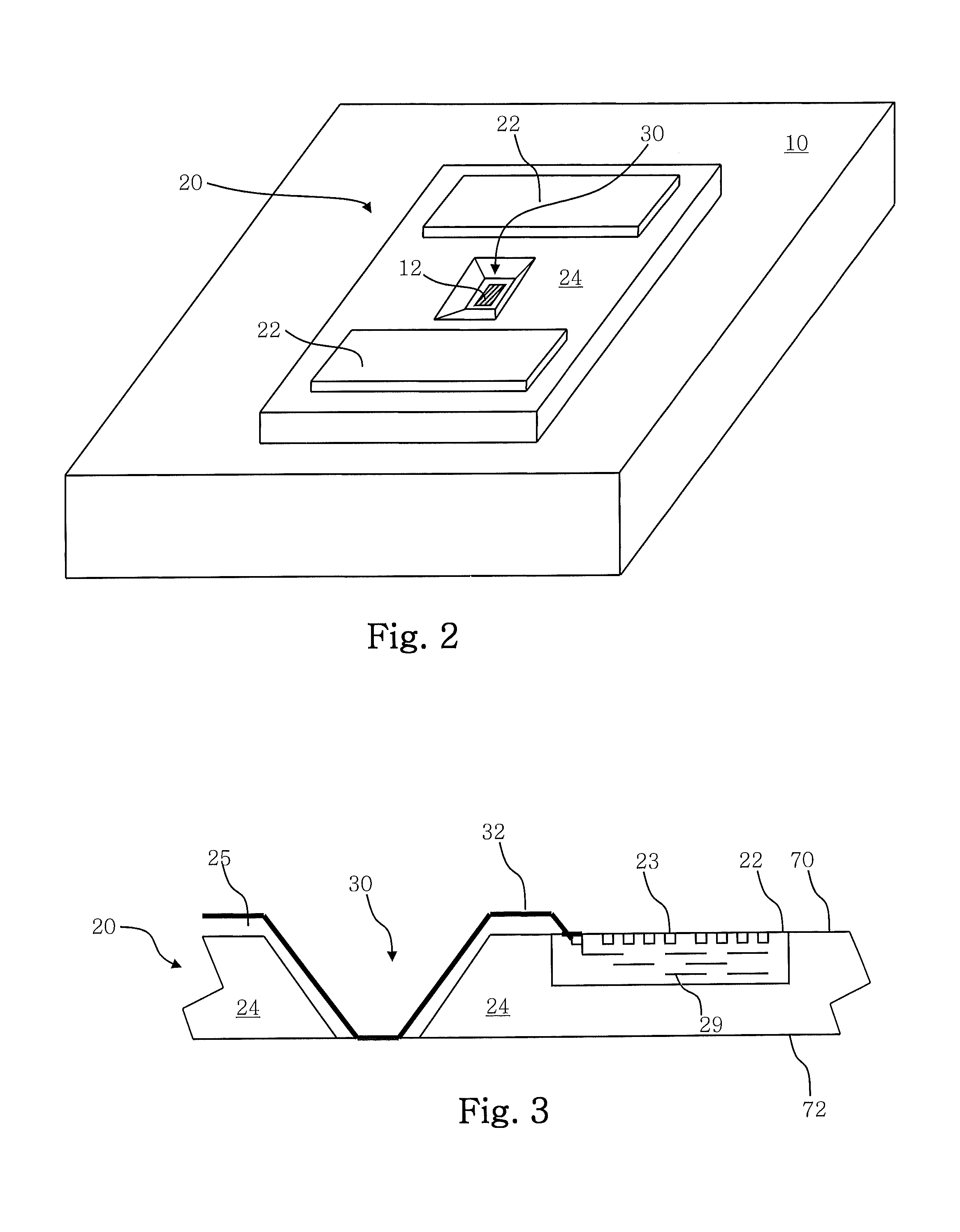
[0095]The present invention now will be described more fully hereinafter with reference to the accompanying drawings, in which embodiments of the invention are shown. However, this invention should not be construed as limited to the embodiments set forth herein. Rather, these embodiments are provided so that this disclosure will be thorough and complete, and will fully convey the scope of the invention to those skilled in the art. In the drawings, the thickness of layers and regions are exaggerated for clarity. Like numbers refer to like elements throughout.

[0096]It will be understood that when an element such as a layer, region or substrate is referred to as being “on” or extending “onto” another element, it can be directly on or extend directly onto the other element or intervening elements may also be present. In contrast, when an element is referred to as being “directly on” or extending “directly onto” another element, there are no intervening elements present. It will also be ...


PUM

PropertyMeasurementUnit
thicknessaaaaaaaaaa
thicknessaaaaaaaaaa
thicknessaaaaaaaaaa

Abstract

An active component array includes a target substrate having one or more contacts formed on a side of the target substrate, and one or more printable active components distributed over the target substrate. Each active component includes an active layer having a top side and an opposing bottom side and one or more active element(s) formed on or in the top side of the active layer. The active element(s) are electrically connected to the contact(s), and the bottom side is adhered to the target substrate. Related fabrication methods are also discussed.

Description

CLAIM OF PRIORITY[0001]The present application is a 35 U.S.C. §371 national phase application of PCT International Application No. PCT / US2011 / 029365, entitled “Electrically Bonded Arrays Of Transfer Printed Active Components”, having an international filing date of Mar. 22, 2011, which claims priority from U.S. Provisional Patent Application No. 61 / 318,522 entitled “Active Backplane,” filed on Mar. 29, 2010 with the United States Patent and Trademark Office, the disclosures of which are incorporated by reference herein in their entireties. The above PCT International Application was published in the English language and has International Publication No. WO 2011 / 126726 A1.FIELD OF THE INVENTION[0002]The present invention is an apparatus and method for providing a target substrate with electrically active components distributed thereon.BACKGROUND OF THE INVENTION[0003]Large substrates with electronically active components distributed over the extent of the substrate may be used in a v...

Claims


Application Information

Patent Timeline
Patent Type & Authority Patents(United States)
IPC IPC(8): H05K7/00H05K1/16B23K31/00H01L21/683H01L21/768H01L23/00H01L23/48H01L27/12H01L27/146H01L31/0203H01L31/048H01S5/02315H05K1/18H05K13/04
CPCH01L24/08H01L24/24H01L24/29H01L24/73H01L24/83H05K1/18H01L21/6835H01L21/76898H01L23/481H01L27/1214H01L27/1266H01L27/14618H01L31/0203H01L31/048H05K13/04H05K13/046H01L2224/24011H01L24/02H01L24/05H01L24/27H01L24/30H01L24/32H01L24/82H01L24/92H01L2221/6835H01L2221/68372H01L2221/68381H01L2224/02371H01L2224/02372H01L2224/0239H01L2224/04026H01L2224/05548H01L2224/056H01L2224/08238H01L2224/24137H01L2224/24147H01L2224/24226H01L2224/245H01L2224/24998H01L2224/2731H01L2224/29078H01L2224/291H01L2224/2919H01L2224/2929H01L2224/29344H01L2224/3012H01L2224/32104H01L2224/32146H01L2224/32227H01L2224/73267H01L2224/76155H01L2224/80203H01L2224/80224H01L2224/821H01L2224/82106H01L2224/83093H01L2224/83121H01L2224/83191H01L2224/83192H01L2224/83805H01L2224/83815H01L2224/8384H01L2224/83851H01L2224/83855H01L2224/83859H01L2224/83862H01L2224/83868H01L2224/83871H01L2224/83874H01L2224/92244H01L2924/01013H01L2924/01029H01L2924/01032H01L2924/01047H01L2924/01049H01L2924/0105H01L2924/01057H01L2924/01079H01L2924/01082H01L2924/10329H01L2924/12044H01S5/02236H01S5/02276H01L2924/01005H01L2924/01006H01L2924/01023H01L2924/01033H01L2924/01075H01L2924/01322H01L2924/014H01L2224/29101H01L2924/0132H01L2924/0133H01L2224/29111Y02E10/50H01L2224/82007H01L2924/15787H01L2224/82102H01L2924/12041H01L2224/92143H01L2224/81192H01L2924/12042H01L2924/14Y10T29/49139Y10T29/4913H01L2924/15153H01S5/0233H01S5/0235H01S5/02345H01S5/02315H01L2924/00014H01L2924/00H01L2224/13111H05K3/10H05K3/0058
Inventor MENARD, ETIENNEBOWER, CHRISTOPHERMEITL, MATTHEWGARROU, PHILIP
Owner X DISPLAY CO TECH LTD
Why Eureka
Try Eureka