Nano piezoelectric device having a nanowire and method of forming the same

a piezoelectric device and nanowire technology, applied in piezoelectric/electrostrictive device details, nanotechnology, piezoelectric/electrostrictive/magnetostrictive devices, etc., can solve the problems of limiting the practical application of the device, low bending tolerance, and difficult deformation significantly, so as to improve mechanical and electrical characteristics

Active Publication Date: 2015-06-16
ELECTRONICS & TELECOMM RES INST
View PDF25 Cites 3 Cited by
  • Summary
  • Abstract
  • Description
  • Claims
  • Application Information

AI Technical Summary

Benefits of technology

[0006]The present invention provides a nano piezoelectric device having improved mechanical and electrical characteristics.

Problems solved by technology

Since the piezoelectric materials (which are in solid state) have a high Young's modulus, they are difficult to deform significantly.
Thus, typical thick-film piezoelectric materials are difficult to miniaturize, and have low bending tolerance, which limit their practical application.
Although these typical bulk or thick-film materials have excellent piezoelectric characteristics, their future applications are limited by their high sintering temperatures of about 600° C. or more, and because the crystalline material is expensive and contains toxic material such as lead.
In addition, these materials have limitations in that they cannot be applied to future portable devices or terminals for ubiquitous services that must be miniaturized and lightweight and to plastic substrates.

Method used


Image

  • Nano piezoelectric device having a nanowire and method of forming the same
  • Nano piezoelectric device having a nanowire and method of forming the same
  • Nano piezoelectric device having a nanowire and method of forming the same

Examples


Embodiment Construction

[0027]Preferred embodiments of the present invention will be described below in more detail with reference to the accompanying drawings. The present invention may, however, be embodied in different forms and should not be constructed as limited to the embodiments set forth herein. Rather, these embodiments are provided so that this disclosure will be thorough and complete, and will fully convey the scope of the present invention to those skilled in the art.

[0028]In the figures, the dimensions of layers and regions are exaggerated for clarity of illustration. Like reference numerals refer to like elements throughout.

[0029]Hereinafter, it will be described about exemplary embodiments of the present invention in conjunction with the accompanying drawings.

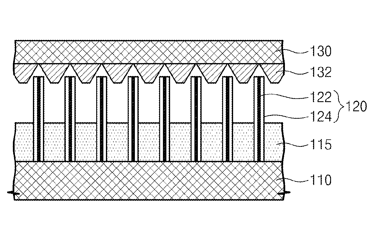
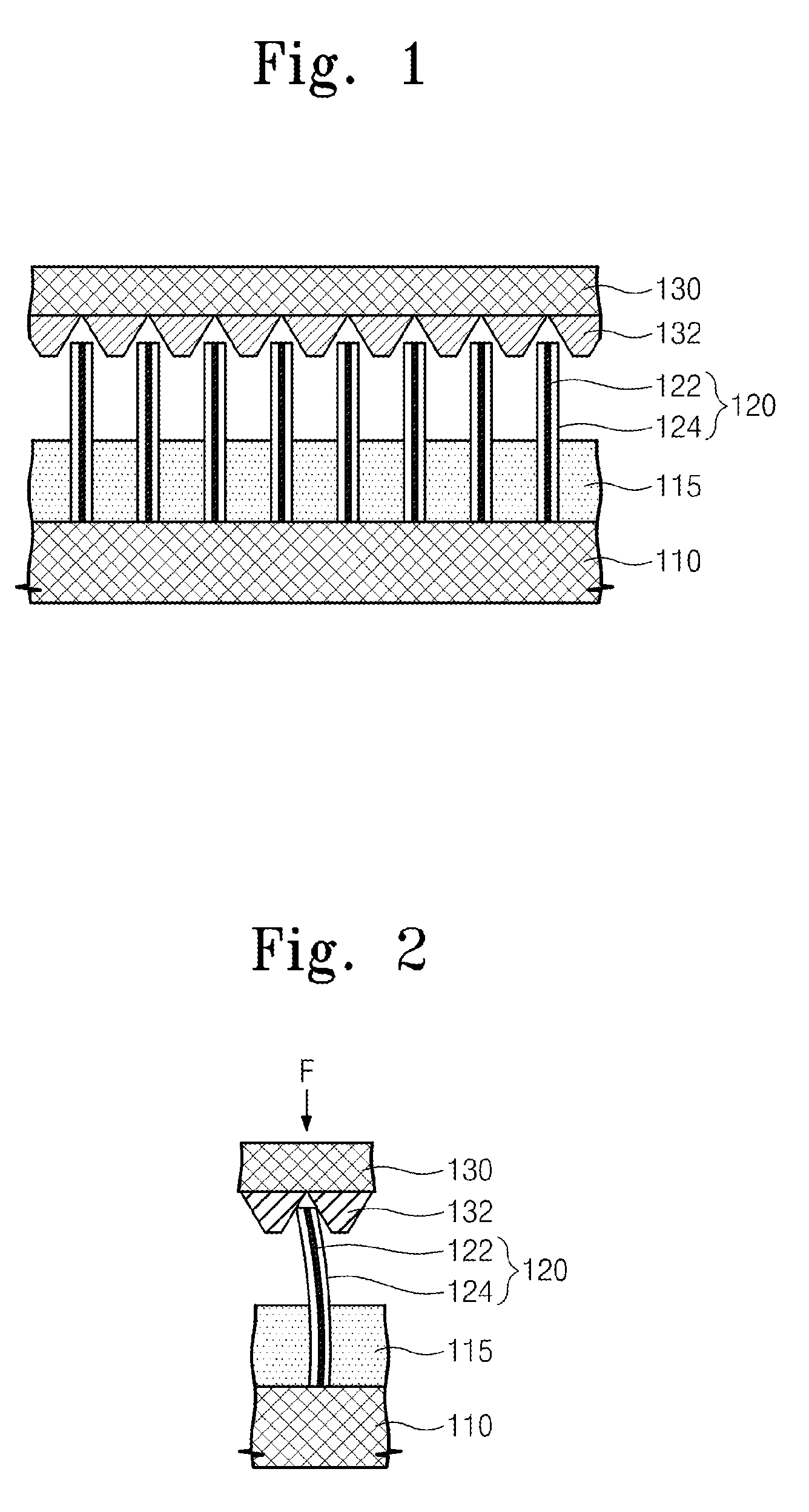
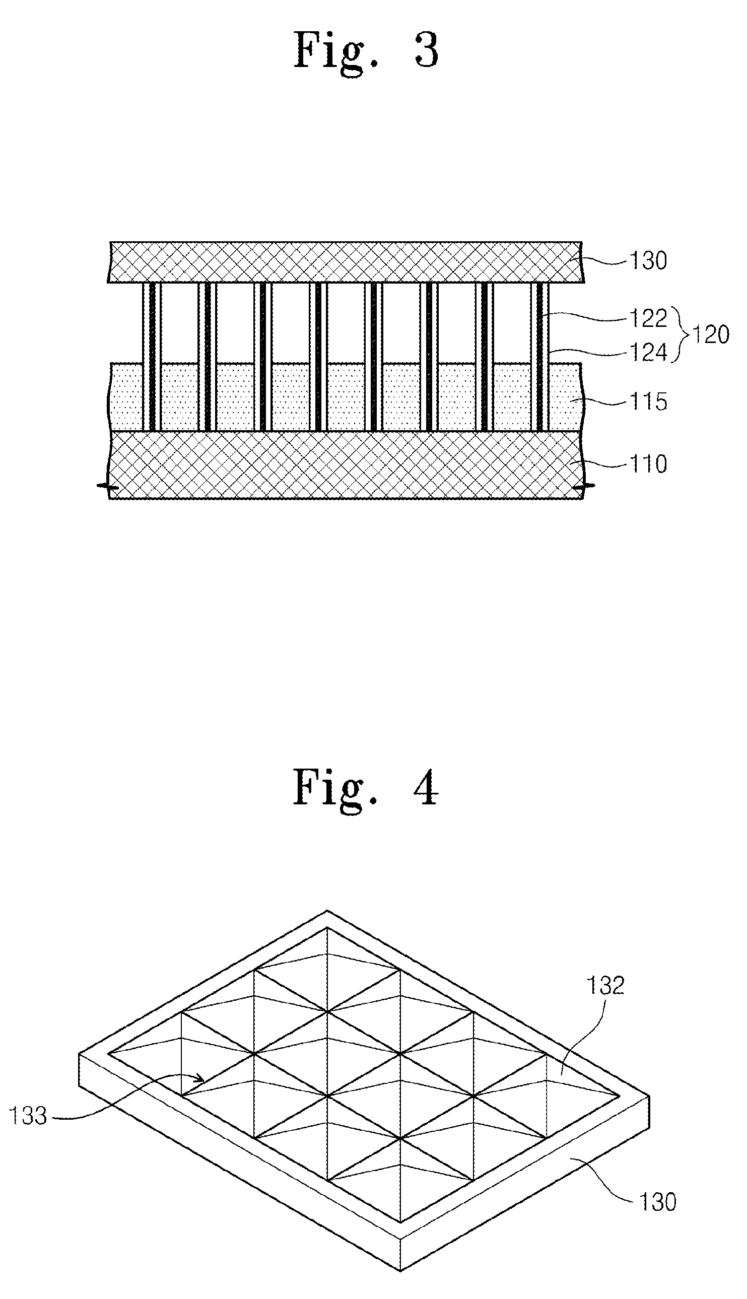
[0030]FIG. 1 is a schematic view illustrating a nano piezoelectric device according to an embodiment of the present invention.

[0031]Referring to FIG. 1, a plurality of nanowires 120 are disposed on a lower electrode 110. Each of the na...


PUM

PropertyMeasurementUnit
diameteraaaaaaaaaa
diameteraaaaaaaaaa
widthaaaaaaaaaa

Abstract

Provided are a nano piezoelectric device and a method of forming the nano piezoelectric device. The nano piezoelectric device includes a lower electrode, a nanowire extending upward from the lower electrode, and an upper electrode on the nanowire. The nanowire includes a conductive wire core and a wire shell surrounding the wire core and including a piezoelectric material.

Description

CROSS-REFERENCE TO RELATED APPLICATIONS[0001]This application is a Continuation-in-part of application Ser. No. 12 / 544,694, filed on Aug. 20, 2009. Furthermore, this application claims the benefit of priority of Korean applications 10-2008-0124014, filed Dec. 8, 2008, and 10-2009-0024626, filed on Mar. 23, 2009. The disclosures of these prior U.S. and Korean applications are incorporated herein by reference.BACKGROUND OF THE INVENTION[0002]The present invention disclosed herein relates to an energy-harvesting device and a method of forming the energy-harvesting device, and more particularly, to a nano piezoelectric device and a method of forming the nano piezoelectric device.[0003]Piezoelectric devices use the piezoelectric principle to convert deformation induced by physical force to electrical energy. Such a piezoelectric device is configured with piezoelectric material disposed between an upper electrode and a lower electrode. When the piezoelectric material between the two elect...

Claims


Application Information

Patent Timeline
Patent Type & Authority Patents(United States)
IPC IPC(8): H01L41/04H01L41/113H01L41/316B82Y15/00
CPCH01L41/316H01L41/1136Y10T29/42B82Y15/00H10N30/306H10N30/076
Inventor PARK, JONG-HYURK
Owner ELECTRONICS & TELECOMM RES INST
Why Eureka
Try Eureka