
Writing method of variable resistance non-volatile memory element and variable resistance non-volatile memory device

a non-volatile memory element and variable resistance technology, applied in the direction of information storage, static storage, digital storage, etc., can solve the problem of unstable resistance changing state, and achieve the effect of improving the reliability of the non-volatile memory device and stable continuation of the resistance changing operation

Active Publication Date: 2015-06-23
PANASONIC SEMICON SOLUTIONS CO LTD
View PDF13 Cites 15 Cited by
  • Summary
  • Abstract
  • Description
  • Claims
  • Application Information

AI Technical Summary

Benefits of technology

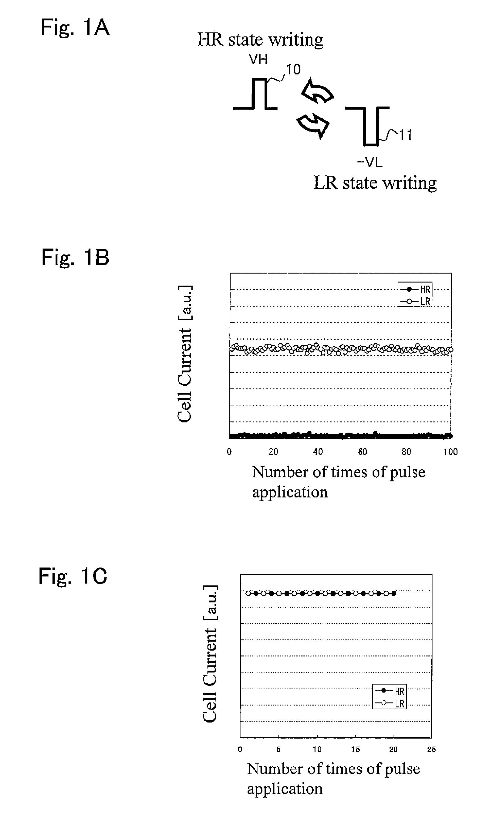
[0008]An object of one non-limiting and exemplary embodiment is to provide a writing method of a variable resistance non-volatile memory element, and a variable resistance non-volatile memory device, which can substantially resolve an unstable resistance changing phenomenon, which occurs in the conventional examples.
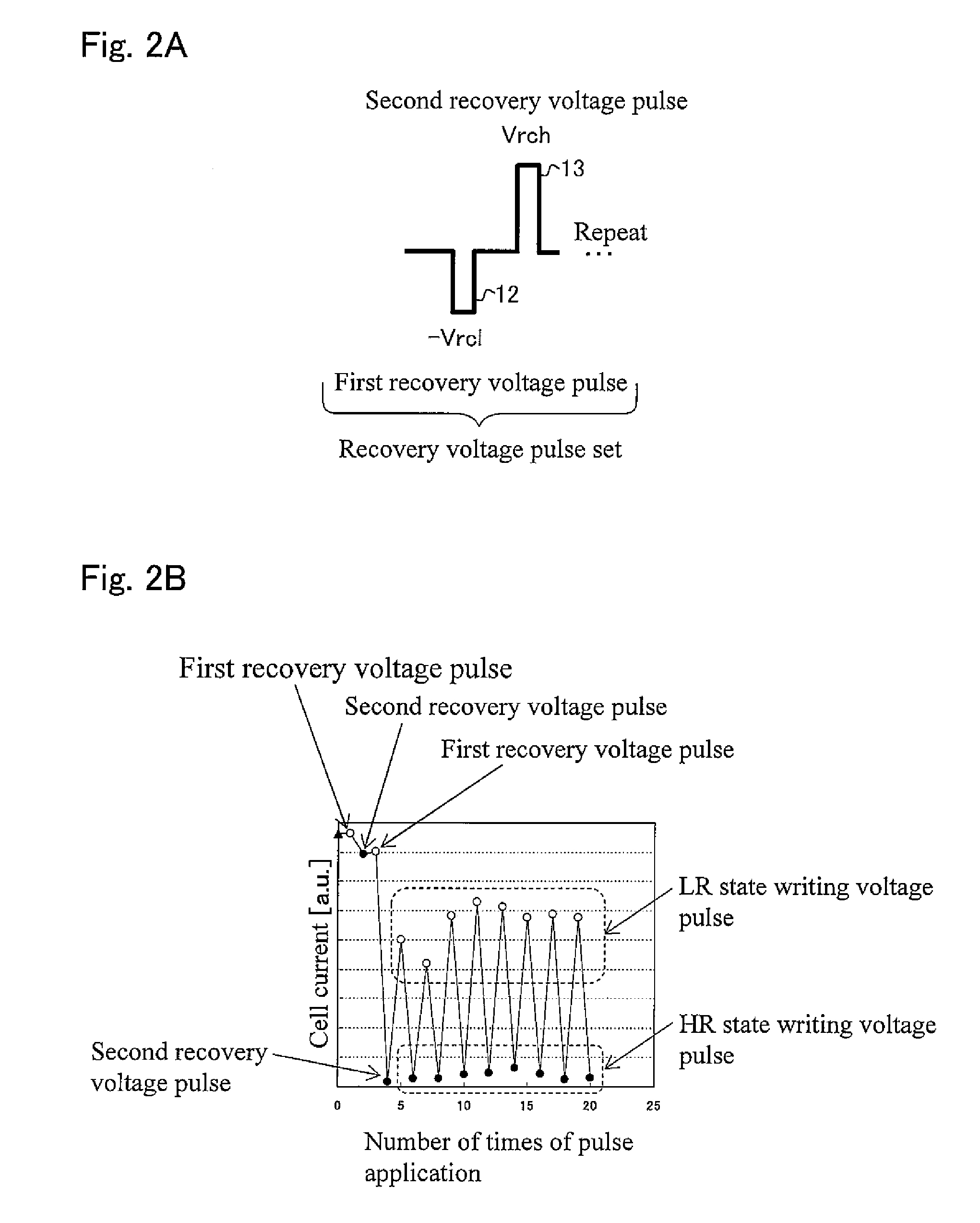
[0011]According to one aspect of the present disclosure, it becomes possible to ensure a proper operation window even when the number of times of rewriting increases. As a result, it becomes possible to stably continue a resistance changing operation, and significantly improve reliability of the non-volatile memory device.

Problems solved by technology

However, when the number of times of rewriting is increased, a resistance changing state becomes unstable.

Method used


Image

  • Writing method of variable resistance non-volatile memory element and variable resistance non-volatile memory device
  • Writing method of variable resistance non-volatile memory element and variable resistance non-volatile memory device
  • Writing method of variable resistance non-volatile memory element and variable resistance non-volatile memory device

Examples


embodiment 1

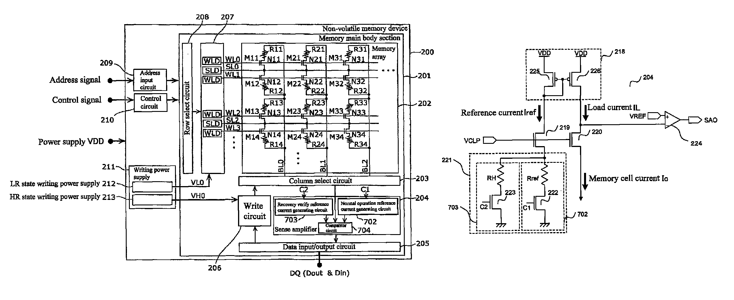
[0070]According to Embodiment 1, there is provided a writing method of a variable resistance non-volatile memory element, in which a voltage pulse is applied to the variable resistance non-volatile memory element to reversibly change a resistance state of the variable resistance non-volatile memory element, the variable resistance non-volatile memory element including a first electrode, a second electrode, and a variable resistance layer sandwiched between the first electrode and the second electrode; the variable resistance layer including a first metal oxide layer which is in contact with the first electrode, and a second metal oxide layer which is in contact with the second electrode and is lower in degree of oxygen deficiency than the first metal oxide layer; the variable resistance non-volatile memory element having a characteristic in which the variable resistance non-volatile memory element changes the resistance state from a first resistance state used to store first informa...


PUM


Abstract

A writing method of a variable resistance non-volatile memory element comprises determining, in a first determination step, whether or not a resistance state of the variable resistance non-volatile memory element does not switch to a first resistance state and remains in a second resistance state, when a pulse of a second voltage is applied to the variable resistance non-volatile memory element; and when it is determined that the resistance state of the variable resistance non-volatile memory element does not switch to the first resistance state and remains in the second resistance state in the first determination step, applying, in a recovery step, at least once to the variable-resistance non-volatile memory element a recovery voltage pulse set composed of two pulses which are a first recovery voltage pulse which has the same polarity as that of the first voltage and a second recovery voltage pulse which has the same polarity as that of the second voltage, has a greater amplitude than the second voltage, and is applied subsequently to the first recovery voltage pulse.

Description

CROSS-REFERENCE TO RELATED PATENT APPLICATION[0001]The application claims priority to Japanese Patent Application No. 2013-077348 filed on Apr. 3, 2013, the entire disclosure of which is incorporated herein by reference.BACKGROUND OF THE DISCLOSURE[0002]1. Field of the Disclosure[0003]The present disclosure relates to a writing method of a variable resistance non-volatile memory element, and a variable resistance non-volatile memory device. More specifically, the present disclosure relates to a writing method of a bipolar variable resistance non-volatile memory element, and a bipolar variable resistance non-volatile memory device.[0004]2. Description of the Related Art[0005]In recent years, a variable resistance non-volatile memory device (hereinafter may be simply referred to as non-volatile memory device) incorporating a memory cell including a variable resistance non-volatile memory element (hereinafter may be simply referred to as variable resistance element) has been studied an...

Claims


Application Information

Patent Timeline
Patent Type & Authority Patents(United States)
IPC IPC(8): G11C11/00G11C13/00
CPCG11C13/0069G11C13/0007G11C13/0064G11C2013/0042G11C2013/0054G11C2213/79
Inventor KAWAI, KENSHIMAKAWA, KAZUHIKOKATOH, YOSHIKAZU
Owner PANASONIC SEMICON SOLUTIONS CO LTD
Learn More