Conductive layer of touch screen

a touch screen and conductive layer technology, applied in the field of touch screens, can solve the problems of high requirements for process and equipment, large amount of industrial waste containing heavy metals, and high requirements for graphical etching process, and achieve the effects of reducing material cost, high yield, and simplifying process

Active Publication Date: 2015-06-23
ANHUI JINGZHUO OPTICAL DISPLAY TECH CO LTD
View PDF12 Cites 0 Cited by
  • Summary
  • Abstract
  • Description
  • Claims
  • Application Information

AI Technical Summary

Benefits of technology

[0019]The above mentioned conductive layer having a structure of metal mesh can be manufactured by imprinting. Comparing to the conventional technology with ITO as conductive layer, the imprinting has advantages of one step formation of the mesh, simplified process and high yield. In addition, the material cost is greatly reduced using metal instead of ITO, since no etching process is used, the conductive material will not be wasted, and it reduces heavy metal emission in the waste liquid.

Problems solved by technology

The graphical etching not only has high requirements in process and equipment, but also wastes a lot of ITO material during etching, and produces large amounts of industrial waste containing heavy metals.

Method used


Image

  • Conductive layer of touch screen
  • Conductive layer of touch screen
  • Conductive layer of touch screen

Examples


Embodiment Construction

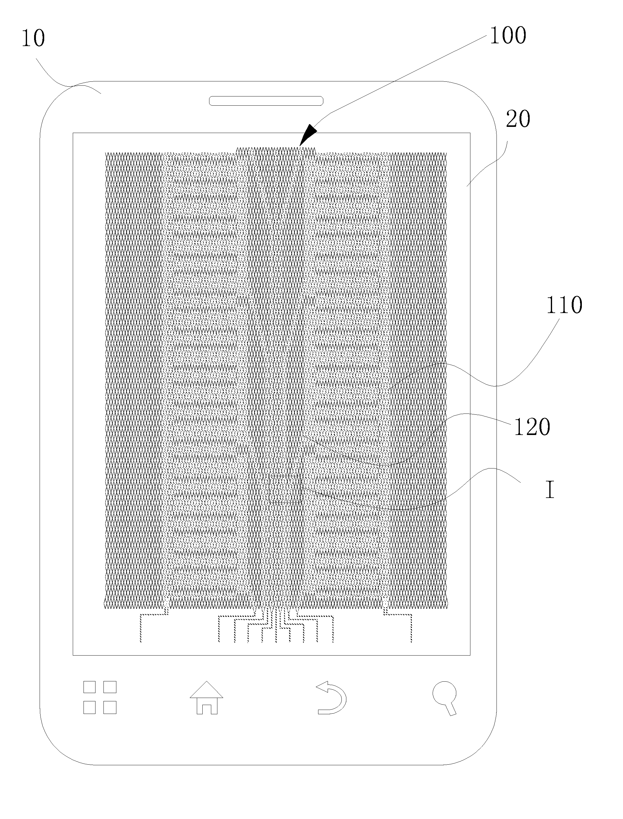
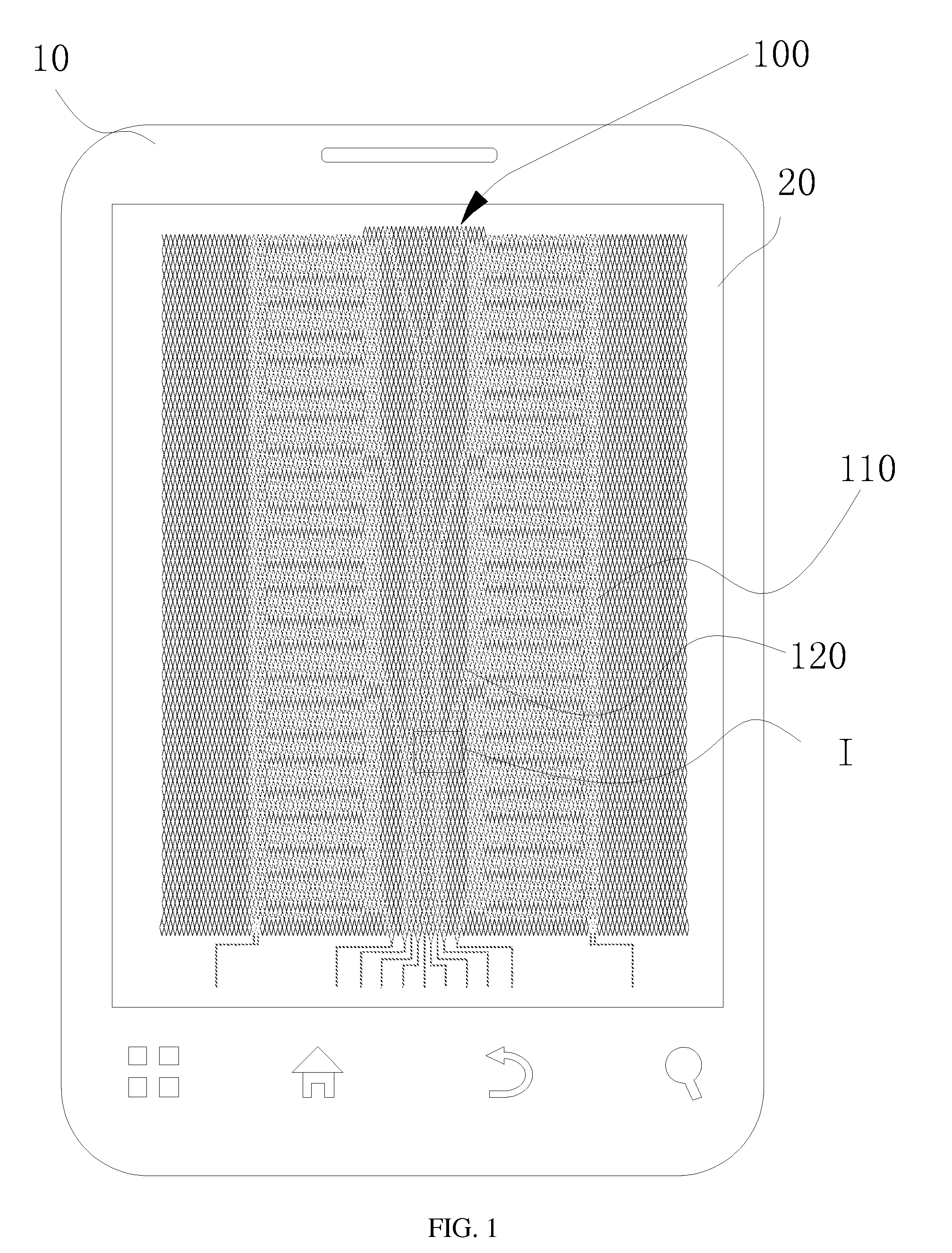
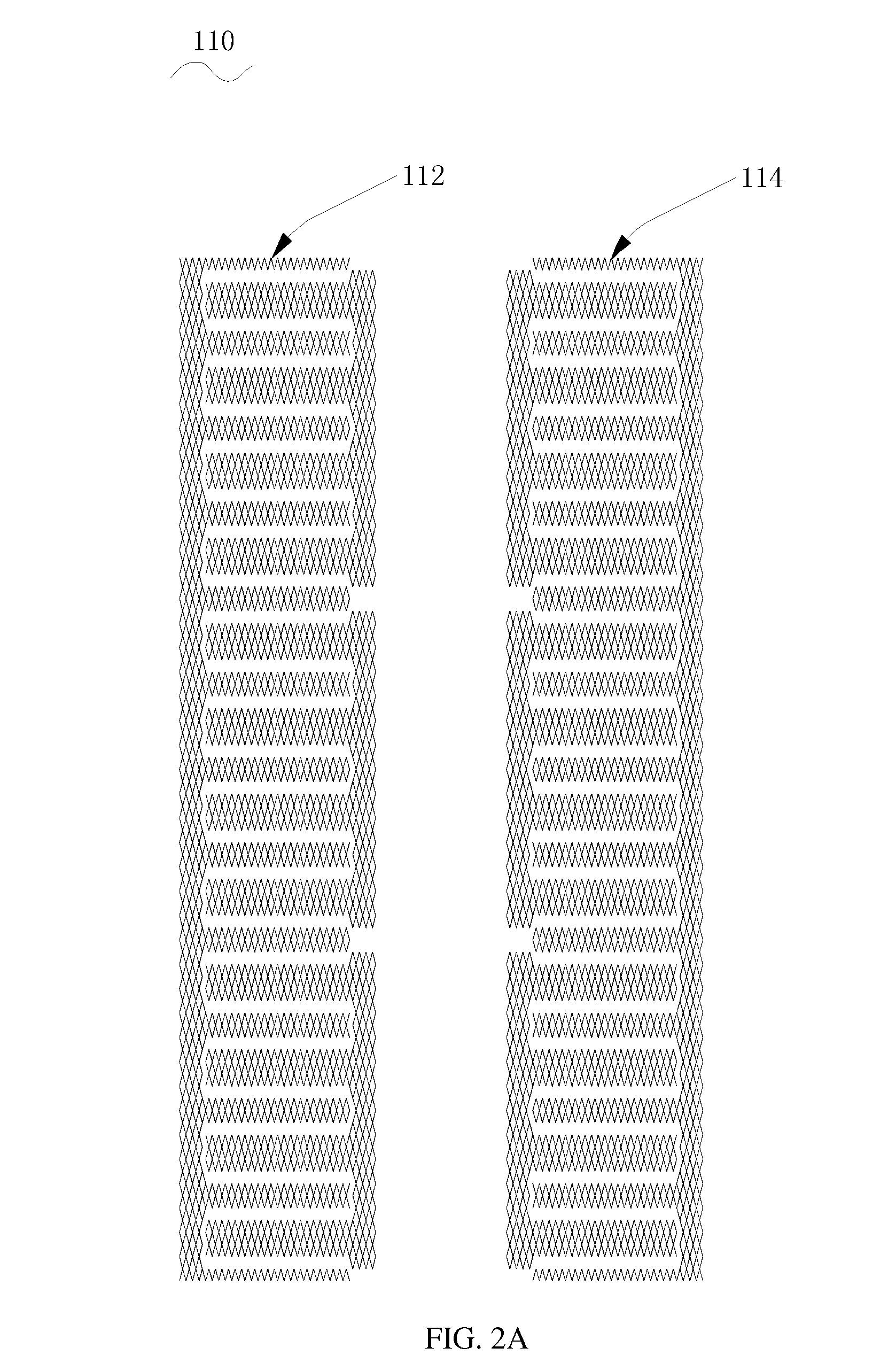
[0030]Illustrative embodiments of the invention are described below. The following explanation provides specific details for a thorough understanding of and enabling description for these embodiments. One skilled in the art will understand that the invention may be practiced without such details. In other instances, well-known structures and functions have not been shown or described in detail to avoid unnecessarily obscuring the description of the embodiments.

[0031]Unless the context clearly requires otherwise, throughout the description and the claims, the words “comprise,”“comprising,” and the like are to be construed in an inclusive sense as opposed to an exclusive or exhaustive sense; that is to say, in the sense of “including, but not limited to.” Words using the singular or plural number also include the plural or singular number respectively. Additionally, the words “herein,”“above,”“below” and words of similar import, when used in this application, shall refer to this appli...


PUM


Abstract

A conductive layer of a touch screen is disclosed including a mesh made of metal wire. The conductive layer includes a sensing area and a wiring area electrically connected to the sensing area, the sensing area includes at least one of the first sensing patterns and at least one of the second sensing patterns, the first sensing pattern and the second sensing pattern are adjacent and electrically insulated from each other, mesh cells in each first sensing pattern are mutually connected, mesh cells in each second sensing pattern are mutually connected. The wiring area includes a plurality of wiring clusters which are mutually insulated, each wiring cluster is formed by interconnecting a column of mesh cells, and one end of each wiring cluster is electrically connected to one of the second sensing patterns. The conductive layer having a structure of metal mesh can be manufactured by imprinting process. Comparing to the conventional technology with ITO film as conductive layer, the imprinting has advantages of one step formation of the mesh, simplified process and high yield rate. In addition, the material cost is greatly reduced using metal instead of ITO, since no etching process is used, the conductive material will not be wasted.

Description

FIELD OF THE INVENTION[0001]The present disclosure relates to touch screens, and more particularly relates to a conductive layer of a touch screen.BACKGROUND OF THE INVENTION[0002]Touch screen is an induction device which can receive touch input signals. The touch screen brings a brand new look to information exchanges and becomes a very appealing new information exchange device. The development of the touch screen technology has drawn a widespread attention from global information media field, and has become an emerged sunrise high-tech industry in optoelectronics industries.[0003]A conductive layer is an essential part of the touch screen. Currently, the conductive layer of the touch screen is Indium Tin Oxide (ITO) formed on an insulative substrate mainly through processes of vacuum plating and graphical etching. The graphical etching not only has high requirements in process and equipment, but also wastes a lot of ITO material during etching, and produces large amounts of indust...

Claims


Application Information

Patent Timeline
Patent Type & Authority Patents(United States)
IPC IPC(8): H05K1/00H05K1/02
CPCH05K1/0296G06F2203/04103G06F2203/04112G06F3/0443H05K1/0274H05K2201/0108H05K2201/09681
Inventor ZHOU, FEI
Owner ANHUI JINGZHUO OPTICAL DISPLAY TECH CO LTD
Why Eureka
Try Eureka