Touch screen and conductive layer thereof

a technology of touch screen and conductive layer, which is applied in the direction of conductive pattern formation, programmable/customizable/modifiable circuits, instruments, etc., can solve the problems of large amount of industrial wastewater, large amount of ito material wasted in etching, etc., and achieves a simple process. , the effect of reducing the cost of material

Active Publication Date: 2015-11-24
ANHUI JINGZHUO OPTICAL DISPLAY TECH CO LTD
View PDF25 Cites 5 Cited by
  • Summary
  • Abstract
  • Description
  • Claims
  • Application Information

AI Technical Summary

Benefits of technology

[0025]The conductive layer of the touch screen has a structure of metal mesh, which can be manufactured by embossing process, compared with the conventional process which uses ITO as a conductive layer, mesh shape can be one-step formed, the process is simple, the yield is high. And the material cost is greatly reduced by using metal instead of ITO, since no etching process is used, the conductive material will not be wasted, and it reduces heavy metal emission in the waste liquid.

Problems solved by technology

Currently, the conductive layer of the touch screen is mostly made of ITO (indium-tin oxide) formed on the insulating substrate through vacuum coating, graphical etching, it is costly on process and equipment, a large number of ITO material will be wasted in etching, and it will produce a large number of industrial wastewater containing heavy metals.

Method used


Image

  • Touch screen and conductive layer thereof
  • Touch screen and conductive layer thereof
  • Touch screen and conductive layer thereof

Examples


Embodiment Construction

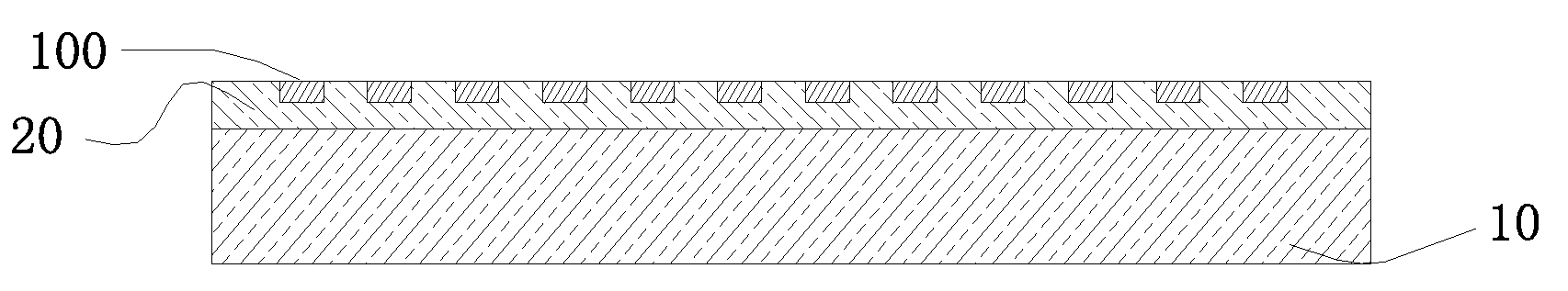
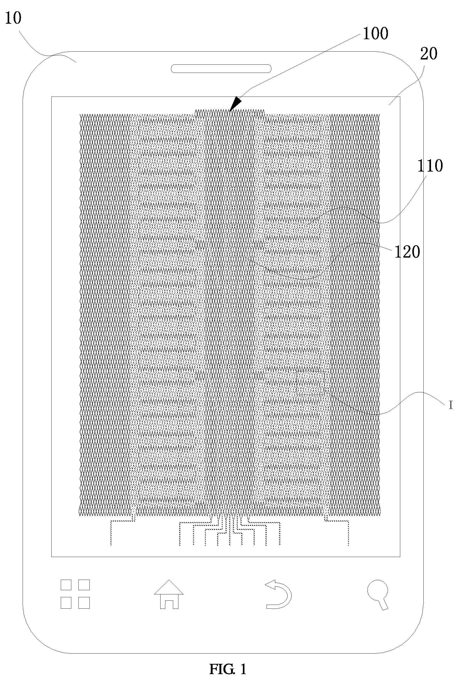
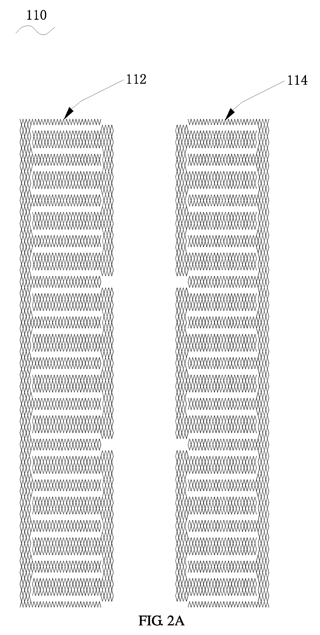
[0035]The invention will be described in detail with the drawings, for easy understanding. The preferred embodiment of the present invention is given in the drawings. However, the present invention can be implemented in different ways, not limited to the embodiments described here. On the contrary, the object of providing these embodiments is to make the content of the invention disclosed more thoroughly and comprehensively.

[0036]It need to be clear, when a component is called “fixed” on another component, it can directly on another component or there can exist component between them. When a component is considered to be “connected” to another component, it can be directly connected to another component or there may exist component between them at the same time. In this paper, the use of the term “vertical”, “horizontal”, “up”, “down”, “left”, “right”, “horizontal”, “vertical” and similar expressions are for illustration purposes only.

[0037]Unless otherwise defined, the technical an...


PUM


Abstract

The present invention relates to a conductive layer of a touch screen. The conductive layer is a mesh composed of metal wires. The mesh comprises a plurality of mesh cells, and the mesh cell comprises a plurality of mesh edges and nodes formed by connecting two adjacent edges. The conductive layer comprises a sensing region and a wire region which is electrically connected to the sensing region. The sensing region comprises a plurality of first sensing patterns and a plurality of second sensing patterns; the first sensing pattern and the second sensing pattern is adjacent and electrically insulated from each other; the mesh cells in each first sensing pattern are electrically connected with each other; and the mesh cells in each second sensing pattern are electrically connected with each other.

Description

FIELD OF THE INVENTION[0001]The present disclosure relates to a touch screen, and more particularly relates to a conductive layer of the touch screen.BACKGROUND OF THE INVENTION[0002]Touch screen is a touch sensor device which can receive input signal. Touch screen gives a new appearance to information interaction, it is a new attractive information interactive device. The development of the touch screen technology causes a widespread concern of the domestic and foreign information media, it becomes a new rising high-tech force in the photoelectric industry.[0003]Conductive layer is a crucially important part of a touch screen. Currently, the conductive layer of the touch screen is mostly made of ITO (indium-tin oxide) formed on the insulating substrate through vacuum coating, graphical etching, it is costly on process and equipment, a large number of ITO material will be wasted in etching, and it will produce a large number of industrial wastewater containing heavy metals.SUMMARY O...

Claims


Application Information

Patent Timeline
Patent Type & Authority Patents(United States)
IPC IPC(8): H05K1/02H05K3/12G06F3/044H05K1/03H05K1/09
CPCH05K1/0296G06F3/044H05K3/1258G06F2203/04103G06F2203/04112H05K1/0289H05K1/0306H05K1/097H05K2201/09681H05K2203/0108G06F3/04164G06F3/0443G06F3/0446G06F3/0448
Inventor ZHOU, FEI
Owner ANHUI JINGZHUO OPTICAL DISPLAY TECH CO LTD
Why Eureka
Try Eureka