Method and system for grating couplers incorporating perturbed waveguides

a technology of perturbed waveguides and grating couplers, applied in the field of semiconductor processing, can solve the problems of cable bulk penalties, considerable power, complex structure, etc., and achieve only modest improvements in reach and limited scalability

Active Publication Date: 2015-07-28
CISCO TECH INC
View PDF9 Cites 38 Cited by
  • Summary
  • Abstract
  • Description
  • Claims
  • Application Information

AI Technical Summary

Problems solved by technology

They can be mitigated to some extent with equalization, coding, and shielding, but these techniques require considerable power, complexity, and cable bulk penalties while offering only modest improvements in reach and very limited scalability.

Method used


Image

  • Method and system for grating couplers incorporating perturbed waveguides
  • Method and system for grating couplers incorporating perturbed waveguides
  • Method and system for grating couplers incorporating perturbed waveguides

Examples


Embodiment Construction

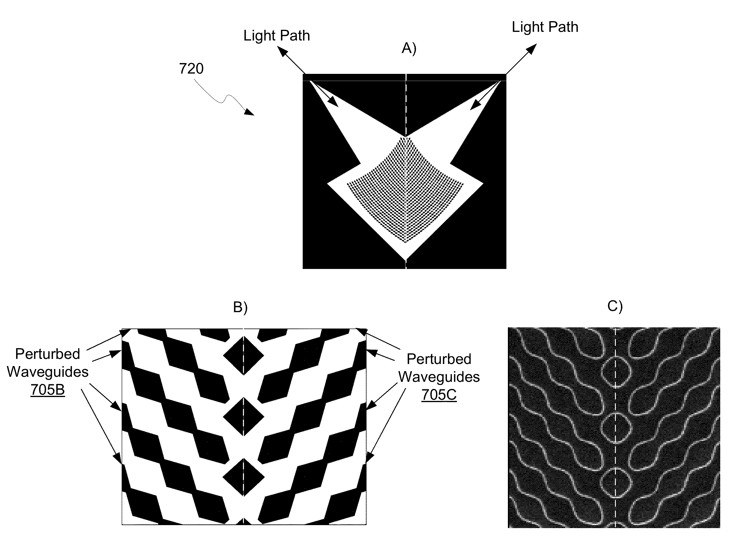
[0029]Certain aspects of the invention may be found in a method and system for grating couplers incorporating perturbed waveguides. Exemplary aspects of the invention may comprise in a semiconductor photonics die, communicating optical signals into and / or out of the semiconductor die utilizing a grating coupler on the semiconductor photonics die, where the grating coupler comprises perturbed waveguides. The perturbed waveguides may comprise a variable width along a length of the perturbed waveguides. The grating coupler may comprise a single polarization grating coupler comprising perturbed waveguides and a non-perturbed grating. The grating coupler may comprise a polarization splitting grating coupler that includes two sets of perturbed waveguides at a non-zero angle from each other. The polarization splitting grating coupler may comprise discrete scatterers at an intersection of the sets of perturbed waveguides. The polarization splitting grating coupler may comprise a plurality o...


PUM


Abstract

Methods and systems for grating couplers incorporating perturbed waveguides are disclosed and may include in a semiconductor photonics die, communicating optical signals into and / or out of the die utilizing a grating coupler on the die, where the grating coupler comprises perturbed waveguides. The perturbed waveguides may comprise a variable width along their length. The grating coupler may comprise a single polarization grating coupler comprising perturbed waveguides and a non-perturbed grating. The grating coupler may comprise a polarization splitting grating coupler (PSCC) that includes two sets of perturbed waveguides at a non-zero angle, or a plurality of non-linear rows of discrete shapes. The PSCC may comprise discrete scatterers at an intersection of the sets of perturbed waveguides. The grating couplers may be etched in a silicon layer on the semiconductor photonics die or deposited on the semiconductor photonics die. The grating coupler may comprise individual scatterers between the perturbed waveguides.

Description

CROSS-REFERENCE TO RELATED APPLICATIONS / INCORPORATION BY REFERENCE[0001]This application claims priority to U.S. Provisional Application 61 / 690,952, filed on Jul. 9, 2012, which is hereby incorporated herein by reference in its entirety.FIELD OF THE INVENTION[0002]Certain embodiments of the invention relate to semiconductor processing. More specifically, certain embodiments of the invention relate to a method and system for grating couplers incorporating perturbed waveguides.BACKGROUND OF THE INVENTION[0003]As data networks scale to meet ever-increasing bandwidth requirements, the shortcomings of copper data channels are becoming apparent. Signal attenuation and crosstalk due to radiated electromagnetic energy are the main impediments encountered by designers of such systems. They can be mitigated to some extent with equalization, coding, and shielding, but these techniques require considerable power, complexity, and cable bulk penalties while offering only modest improvements in re...

Claims


Application Information

Patent Timeline
Patent Type & Authority Patents(United States)
IPC IPC(8): G02B6/34G02B6/42G02B6/124
CPCG02B6/4214G02B6/124G02B6/34G02B5/1861G02B6/26G02B6/30G02B2006/12107
Inventor VERSLEGERS, LIEVENMEKIS, ATTILA
Owner CISCO TECH INC
Why Eureka
Try Eureka