Semiconductor device

a technology of semiconductor devices and semiconductor elements, applied in the direction of oscillator generators, pulse techniques, electronic switching, etc., can solve the problems of uneven placement of moving ions in the insulating film, and reducing so as to prevent the change of characteristics of the semiconductor element and the withstand voltage of the semiconductor devi

Active Publication Date: 2015-08-04
DENSO CORP
View PDF9 Cites 2 Cited by
  • Summary
  • Abstract
  • Description
  • Claims
  • Application Information

AI Technical Summary

Benefits of technology

[0006]It is an object of the present teachings to provide a technique for suppressing the decline in the withstand voltage of the semiconductor device by controlling movement of the movable ions in the insulating film.
[0008]With the semiconductor device described above, since the at least one electrode disposed on the surface of the insulating film is electrically insulated from the semiconductor substrate, the voltage applying circuit is able to apply the first voltage that is independent from the semiconductor substrate to the at least one electrode. Therefore, by adjusting the first voltage that is applied to the at least one electrode, a desired voltage can be applied to the insulating film to control a movement of movable ions in the insulating film. Consequently, even if the movable ions become unevenly located at a particular portion in the insulating film, the movable ions can be dispersed within the insulating film by applying the first voltage to the at least one electrode. Accordingly, a decline in a withstand voltage of the semiconductor device can be prevented. In addition, the voltage applying circuit applies the first voltage to the at least one electrode during the first period in which the second voltage is not applied to the semiconductor element. This in other words may be termed as a period in which the semiconductor element is not driven. Therefore, by applying the first voltage to the at least one electrode, a change in characteristics of the semiconductor element can be prevented.

Problems solved by technology

Therefore, when the semiconductor device is driven and a voltage is applied to the semiconductor substrate, the voltage causes the movable ions to move in the insulating film and become unevenly located at a particular portion in the insulating film.
The movable ions unevenly located at the particular portion in the insulating film affect the withstand voltage structure and reduces the withstand voltage of the semiconductor device.

Method used


Image

  • Semiconductor device
  • Semiconductor device
  • Semiconductor device

Examples


first embodiment

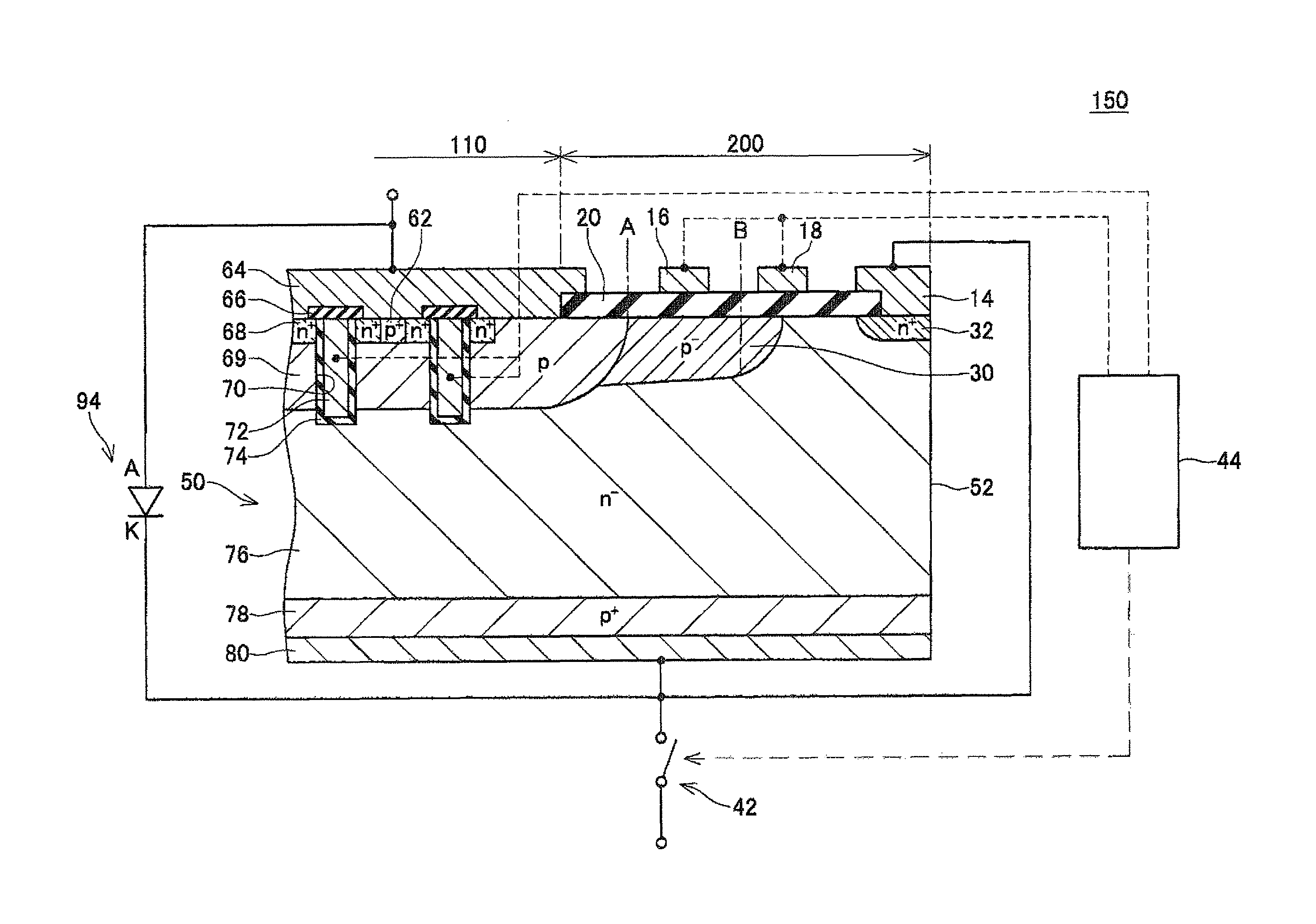
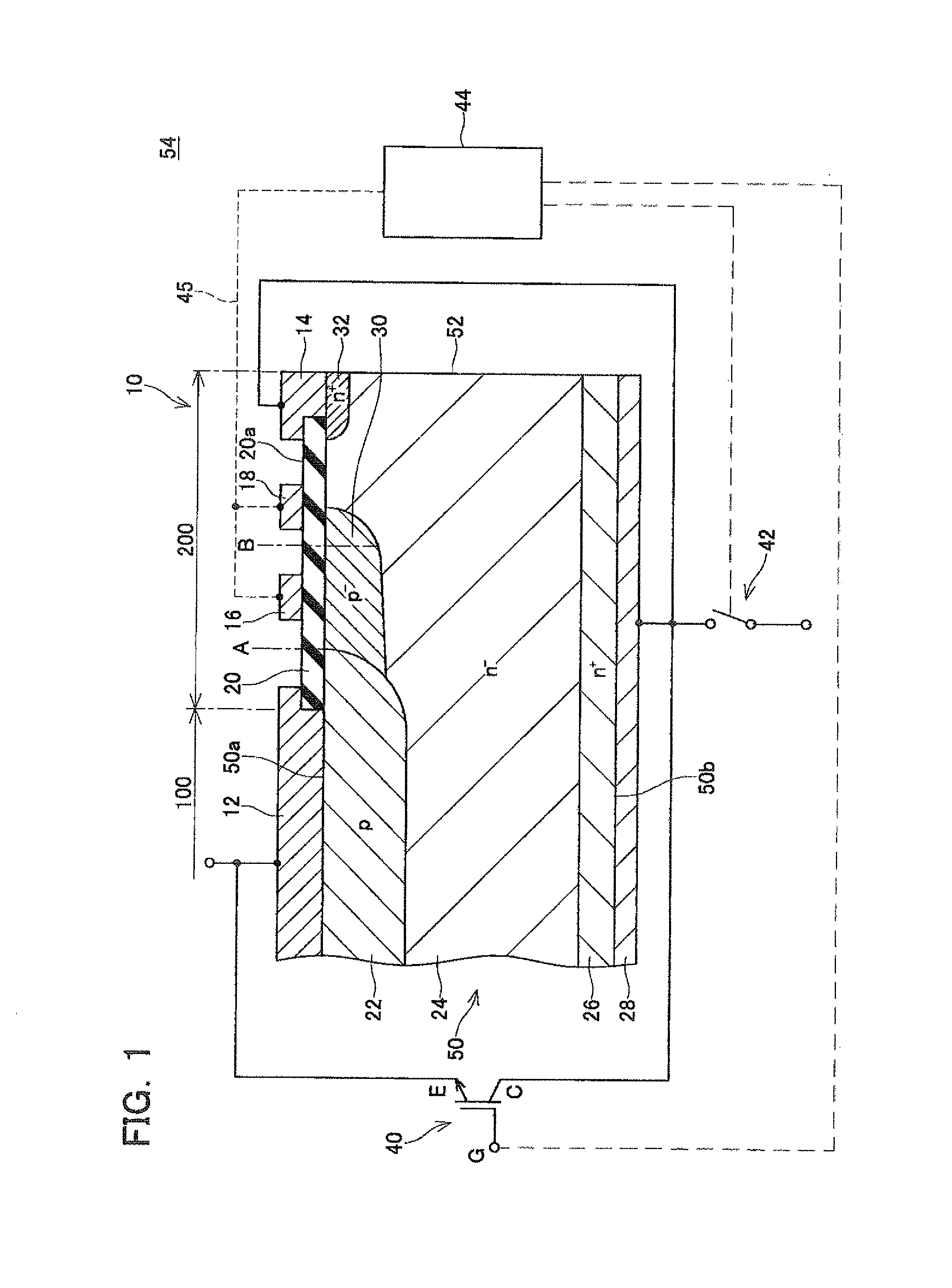
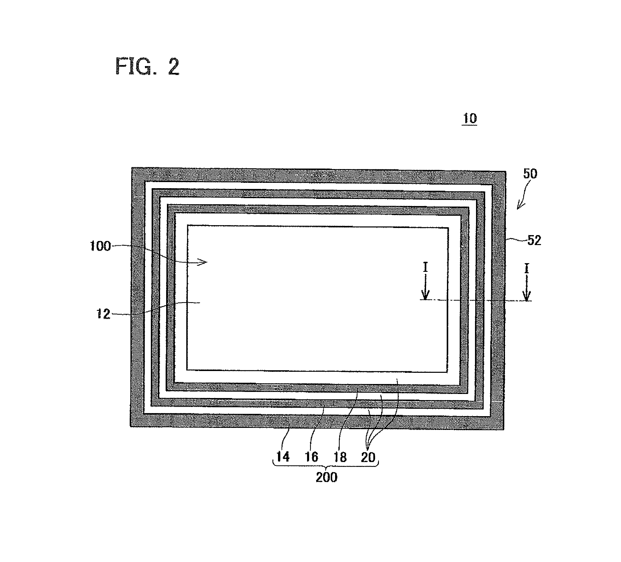
[0022]Hereinafter, an embodiment will be described with reference to the drawings. A semiconductor device 54 according to the present embodiment is a power converter (inverter) which is mounted to a vehicle such as an automobile and which converts inputted DC power into AC power and supplies the AC power to a motor. As shown in FIG. 1, the semiconductor device 54 comprises an IGBT (Insulated Gate Bipolar Transistor) 40, a diode 10, a switch 42, and a drive circuit 44 (corresponding to an example of a voltage applying circuit according to the claims). While the semiconductor device 54 comprises a plurality of switching circuits comprising the IGBT 40 and the diode 10, only one set of the IGBT 40 and the diode 10 is shown in FIG. 1. In addition, among the respective components of the semiconductor device 54, since the IGBT 40 is similar to an IGBT used in a conventional power converter (inverter), a detailed description thereof will be omitted.

[0023]The IGBT 40 is a switching element ...


PUM


Abstract

A semiconductor device may be provided with a semiconductor substrate, an insulating film disposed on a surface of the semiconductor substrate, at least one electrode disposed on a surface of the insulating film, and a voltage applying circuit configured to apply a first voltage to the at least one electrode. The semiconductor substrate may be provided with a cell region and a non-cell region adjacent to the cell region. The cell region is provided with a semiconductor element, and the non-cell region is provided with a withstand voltage structure. The insulating film may be disposed on a surface of the non-cell region. The at least one electrode may be electrically insulated from the semiconductor substrate. The voltage applying circuit may apply the first voltage to the electrode during at least a part of a first period in which a second voltage is not applied to the semiconductor element.

Description

CROSS-REFERENCE TO RELATED APPLICATION[0001]This application claims priority to Japanese Patent Application No. 2011-205745 filed on Sep. 21, 2011, the contents of which are hereby incorporated by reference into the present application.TECHNICAL FIELD[0002]The present teachings relate to a semiconductor device.DESCRIPTION OF RELATED ART[0003]Semiconductor devices have been proposed in which a withstand voltage structure (for example, an FLR (Field Limiting Ring) structure or a RESURF (REduced SURface Field) structure) is formed on a semiconductor substrate in order to increase a withstand voltage of the semiconductor device. With the semiconductor device comprising the withstand voltage structure, an adhesion of movable ions to an insulating film on a surface of a semiconductor substrate may cause a decline in the withstand voltage. Therefore, a technique has been proposed for preventing the decline in the withstand voltage due to the adhesion of the movable ions (Japanese Patent Ap...

Claims


Application Information

Patent Timeline
Patent Type & Authority Patents(United States)
IPC IPC(8): H03K17/00H01L29/06H01L29/861H01L29/739H01L29/40H01L29/10
CPCH03K17/00H01L29/063H01L29/0615H01L29/1095H01L29/402H01L29/404H01L29/7397H01L29/8611H01L29/0638H01L29/0692
Inventor SAITO, JUNHIROSE, MASUHISA
Owner DENSO CORP
Why Eureka
Try Eureka