
Method of manufacturing a conductive via in an organic light emitting display

a technology of organic light emitting display and conductive via, which is applied in the direction of electric lighting sources, solid-state devices, and light sources. it can solve the problems of limit the number of materials that can be used, and impose limits on the methods of manufacturing organic light emitting displays, so as to prevent or reduce brightness. the effect of deterioration

Active Publication Date: 2015-09-08
SAMSUNG DISPLAY CO LTD
View PDF7 Cites 1 Cited by
  • Summary
  • Abstract
  • Description
  • Claims
  • Application Information

AI Technical Summary

Benefits of technology

[0010]Aspects of embodiments of the present invention provide a method of manufacturing an organic light emitting display which is capable of preventing a voltage drop from occurring in a voltage applied to a cathode electrode.
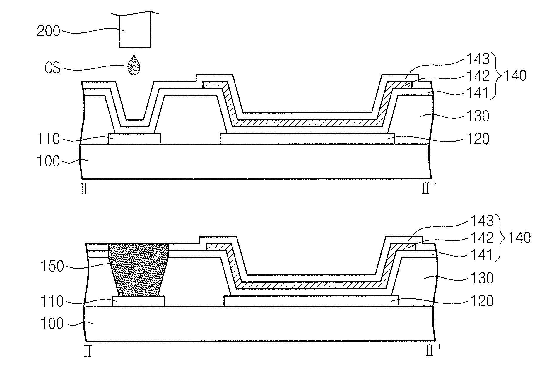
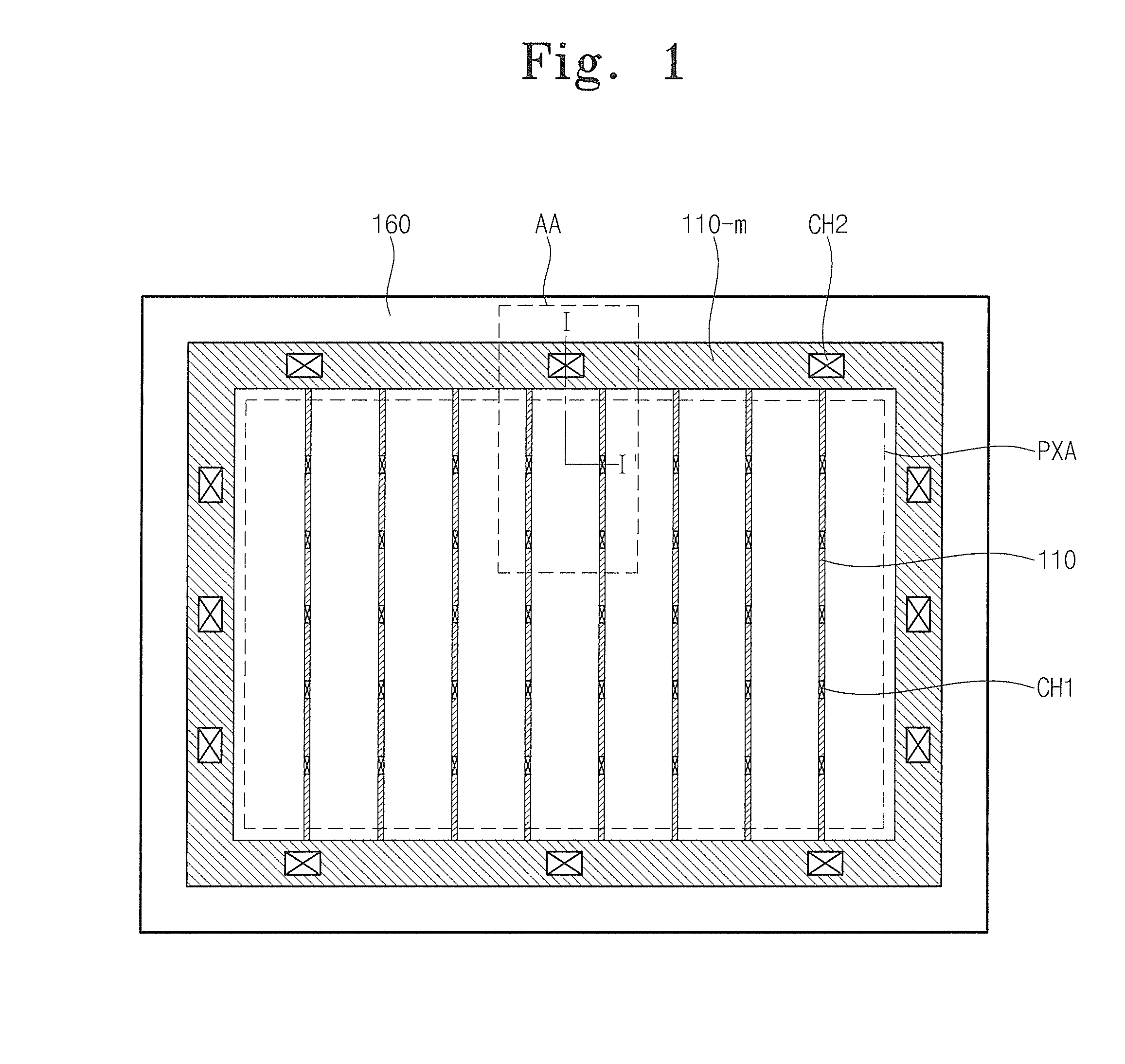
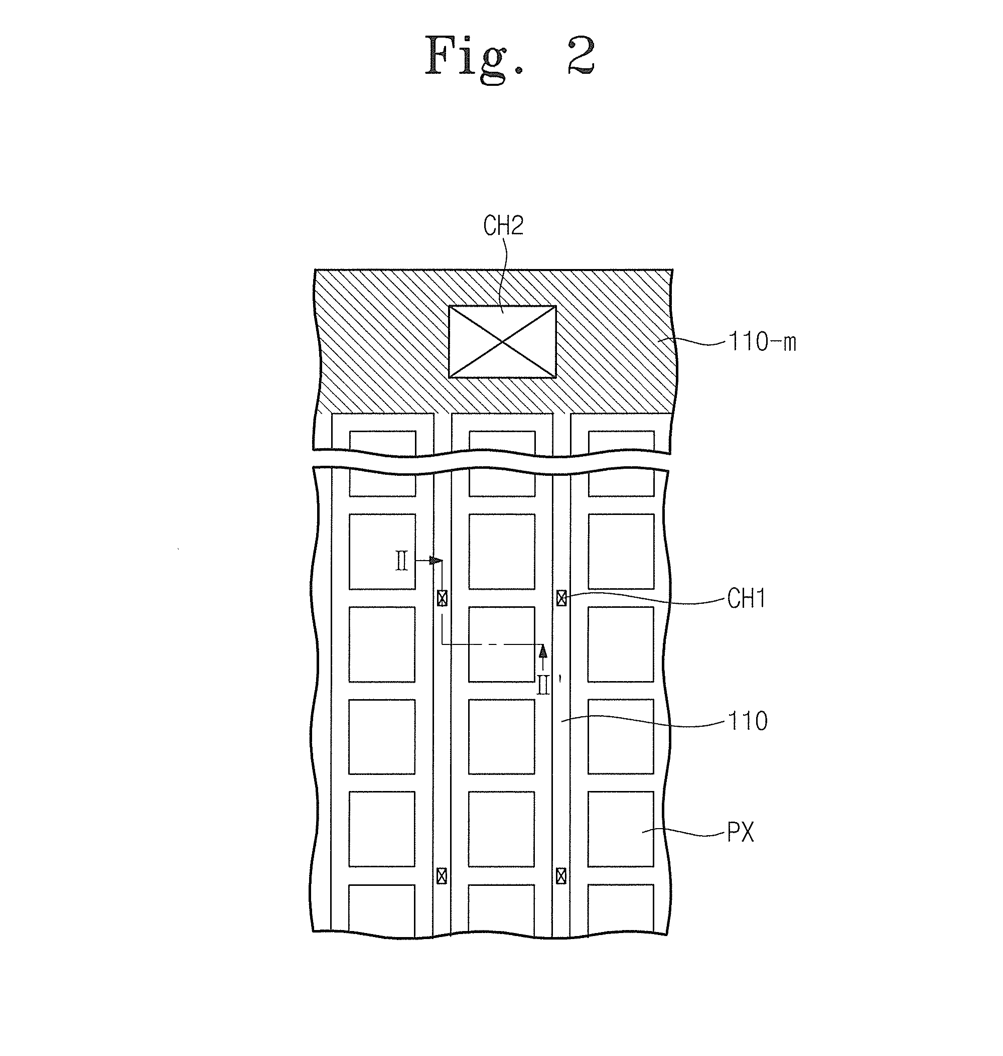
[0021]According to the above, the cathode line is disposed on the substrate and the contact hole is formed in a display area. The electrical connection portion is disposed in the electrical connection portion to electrically connect the cathode line to the cathode electrode, and thus the cathode voltage may be substantially uniformly applied to the whole surface of the display device. Therefore, the display device may prevent or reduce deterioration of brightness.

Problems solved by technology

However, there are a limited number of materials that can be used as a low resistance cathode electrode using the conductive material that is also transparent.
In addition, a rear surface resonance structure is suggested to prevent or reduce deterioration of brightness due to the voltage drop of the cathode electrode, but such a structure imposes limits on the methods of manufacturing the organic light emitting display.

Method used


Image

  • Method of manufacturing a conductive via in an organic light emitting display
  • Method of manufacturing a conductive via in an organic light emitting display
  • Method of manufacturing a conductive via in an organic light emitting display

Examples


Embodiment Construction

[0028]It will be understood that when an element or layer is referred to as being “on”, “connected to” or “coupled to” another element or layer, it can be directly on, connected or coupled to the other element or layer or intervening elements or layers may be present. In contrast, when an element is referred to as being “directly on,”“directly connected to” or “directly coupled to” another element or layer, there are no intervening elements or layers present. Like numbers refer to like elements throughout. As used herein, the term “and / or” includes any and all combinations of one or more of the associated listed items.

[0029]It will be understood that, although the terms first, second, etc. may be used herein to describe various elements, components, regions, layers and / or sections, these elements, components, regions, layers and / or sections should not be limited by these terms. These terms are only used to distinguish one element, component, region, layer, or section from another re...


PUM


Abstract

A manufacturing method of an organic light emitting display includes preparing a substrate including a cathode line and forming an anode electrode on the substrate, the anode electrode being insulated from the cathode line. The method also includes forming an insulating layer having a first opening exposing a portion of the cathode line and a second opening exposing a portion of the anode electrode on the substrate, forming an organic layer on the insulating layer, and forming an electrical connection portion electrically connected to the cathode line. The electrical connection portion is formed in this method by supplying a conductive solution that dissolves the organic layer in an area of the organic layer corresponding to the first opening, and the manufacturing method also includes forming a cathode electrode overlapping with the electrical connection portion.

Description

CROSS-REFERENCE TO RELATED APPLICATION[0001]This patent application claims priority to and the benefit of Korean Patent Application No. 10-2013-0043784, filed on Apr. 19, 2013, the contents of which are hereby incorporated by reference in its entirety.BACKGROUND[0002]1. Field[0003]Aspects of embodiments of the present invention relate to a method of manufacturing an organic light emitting display. More particularly, embodiments of the present invention relate to a method of manufacturing an organic light emitting display which is capable of preventing a voltage applied to a cathode electrode from dropping down.[0004]2. Description of the Related Art[0005]An organic light emitting display includes an anode electrode, a cathode electrode, and an organic material disposed between the anode electrode and the cathode electrode to display an image. Among display devices, the organic light emitting display has been spotlighted as a next generation display device because it has properties, ...

Claims


Application Information

Patent Timeline
Patent Type & Authority Patents(United States)
IPC IPC(8): H01L51/56H01L51/52H01L51/00
CPCH01L51/56H01L51/0017H01L51/0021H01L51/0022H01L51/0023H01L51/5221H10K71/231H10K71/611H10K71/621H10K59/131H10K50/828H10K71/00H05B33/10H10K50/82H10K71/60
Inventor KIM, SUNG WOONG
Owner SAMSUNG DISPLAY CO LTD
Learn More