Dual low voltage levels for control of transfer switch device in pixel array

a transfer switch and low voltage technology, applied in the field of image sensors, can solve the problems of leakage current likely to affect neighboring pixels, and achieve the effect of less charge, reduced blooming problem, and suppressed leakage curren

Active Publication Date: 2015-09-22
HIMAX IMAGING LIMITED
View PDF3 Cites 1 Cited by
  • Summary
  • Abstract
  • Description
  • Claims
  • Application Information

AI Technical Summary

Benefits of technology

[0006]Therefore, one objective of the present invention is to provide an image sensor that can avoid the bloom issue.
[0007]Another objective of the present invention is to provide a pixel array that can avoid the bloom issue.
[0010]In view of above-mentioned embodiments, the control terminals for the long exposure pixel and the short exposure pixel are asserted to a higher level before the data in the pixels are read. Therefore the photo diode accumulates less charge and the leakage current is suppressed. By this way, the bloom issue can be reduced.

Problems solved by technology

If the light is too bright, however, a large quantity of charges are generated and accumulated in the photodiode, and leakage current may likely occur to affect the neighboring pixels.

Method used


Image

  • Dual low voltage levels for control of transfer switch device in pixel array
  • Dual low voltage levels for control of transfer switch device in pixel array
  • Dual low voltage levels for control of transfer switch device in pixel array

Examples


Embodiment Construction

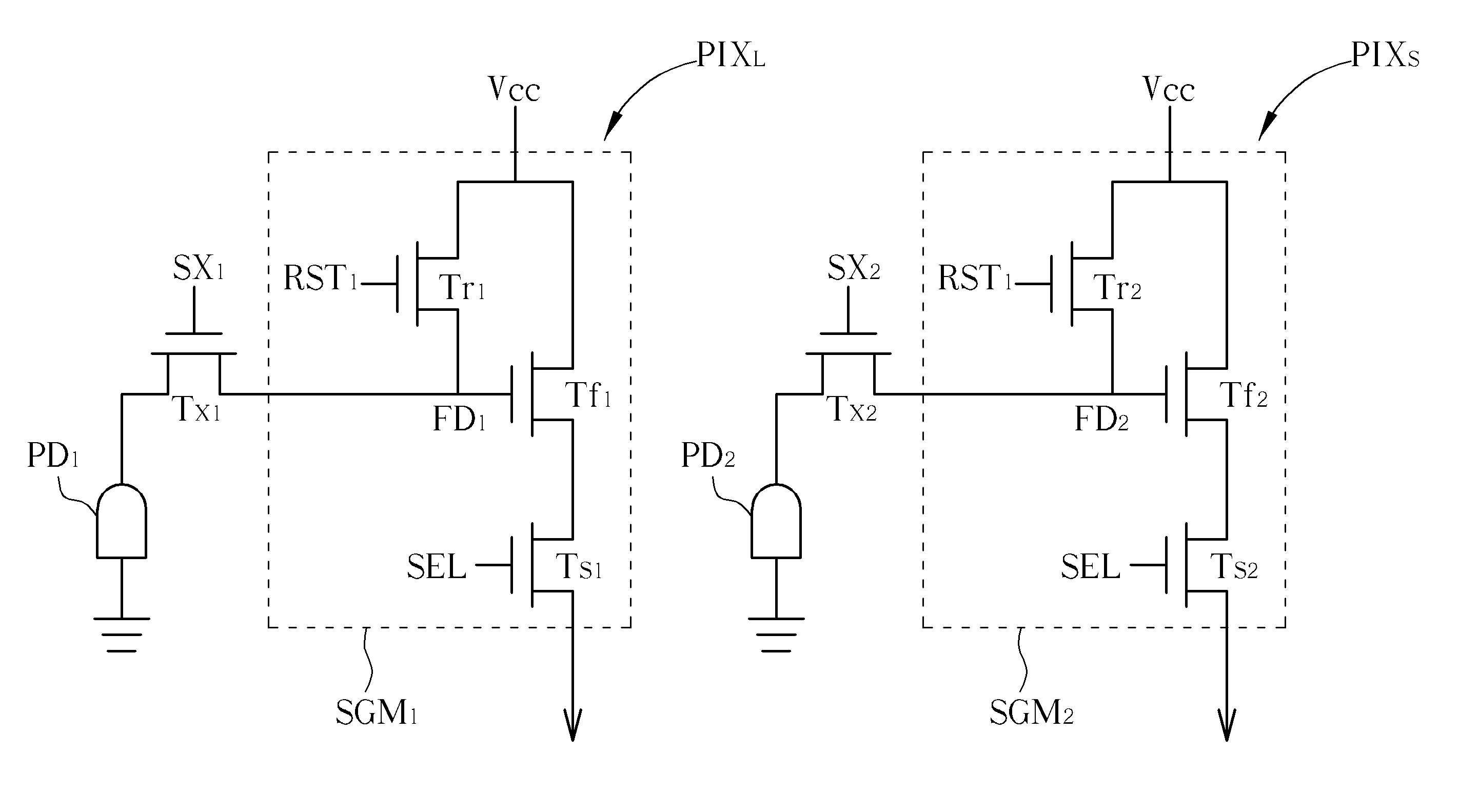
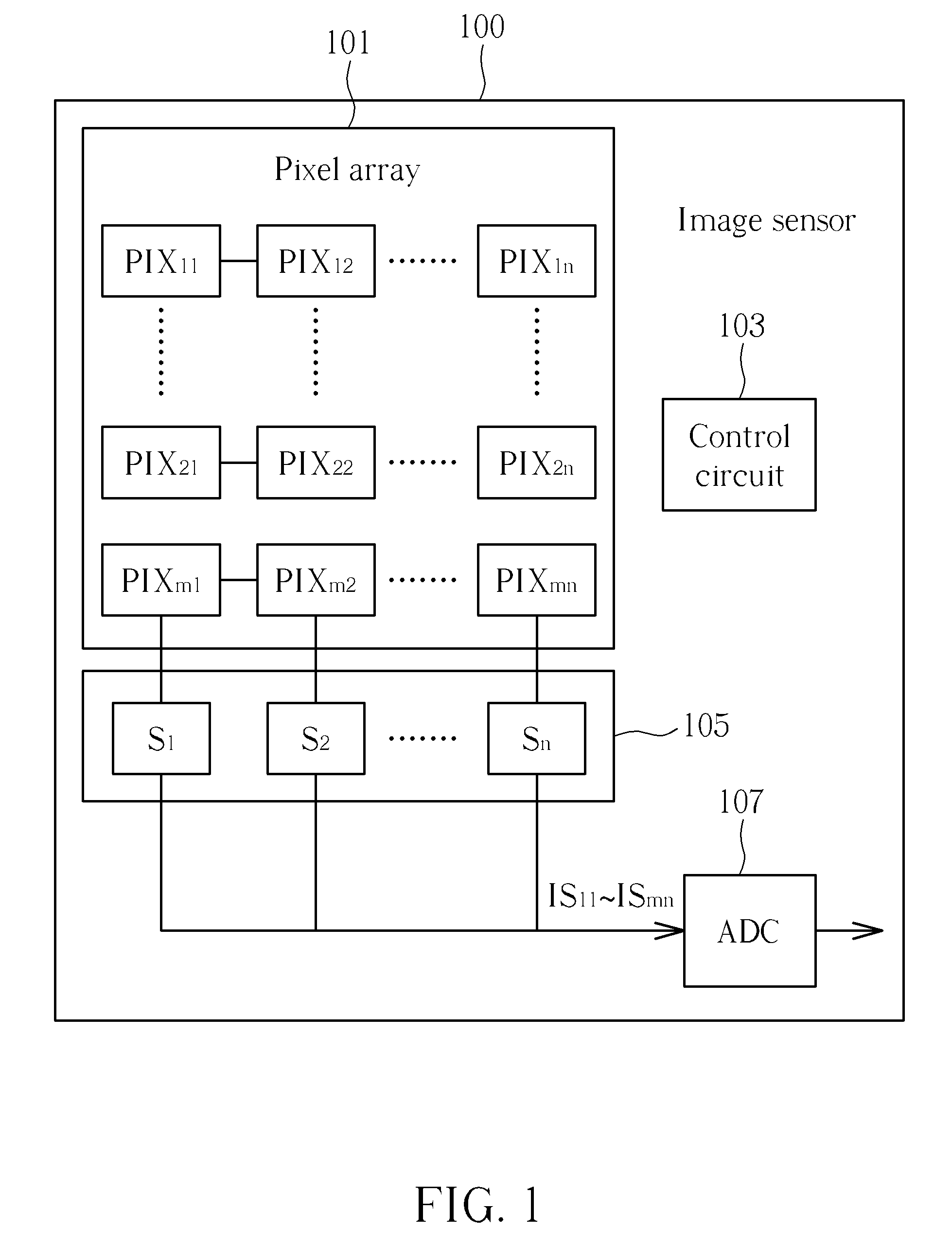
[0017]FIG. 1 is a block diagram illustrating an image sensor 100 according to an embodiment of the present invention. As shown in FIG. 1, the image sensor 100 comprises a pixel array 101, a control circuit 103, a read circuit 105 and an analog to digital converter 107. The pixel array 101 comprises a plurality of pixels PIX11-PIXmn to generate the image signals IS11-ISmn. The read circuit 105 comprises a plurality of read units S1-Sn, which are arranged to read image signals IS11-ISmn from the pixels PIX11-PIXmn. The analog to digital converter 107 generates a frame according the image signals IS11-ISmn. The control circuit 103 controls the operations for each device in the image sensor 100. That is, the control circuit 103 can control the reset time, the exposure time and the read operation for the pixels PIX11-PIXmn.

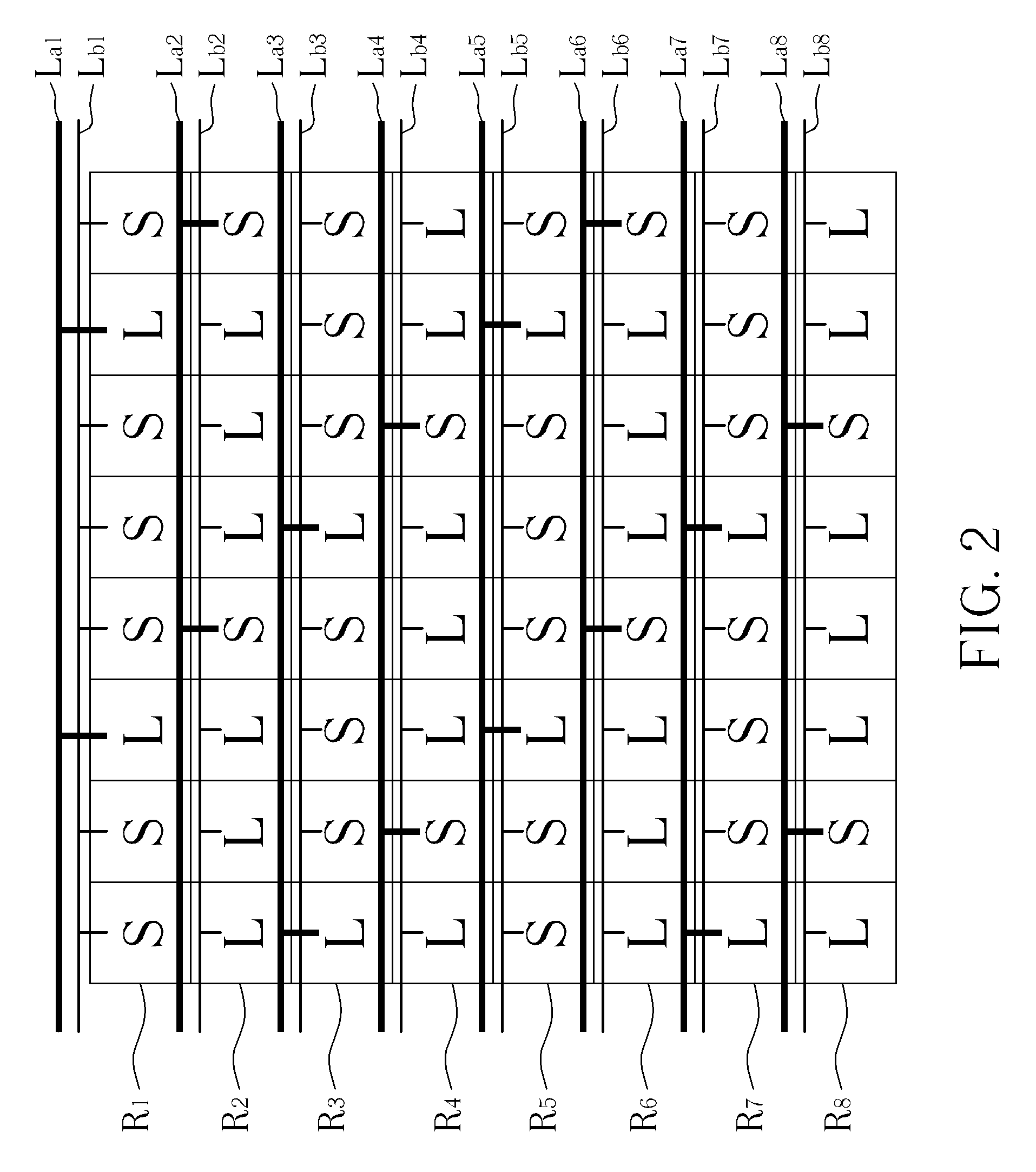
[0018]The pixel array in an image sensor, in one embodiment, may have long exposure pixels and short exposure pixels, such that a high dynamic range (HDR) image is gen...


PUM


Abstract

A pixel array comprises at least one long exposure pixel, short exposure pixel, and a control circuit. The long exposure pixel comprises a first photodiode to generate charges, a first image signal generating module for generating a first image sensing signal; and a first transfer switch device for passing the charges to the first image signal generating module via a first transfer control signal. The control circuit sets the first transfer control signal to be a first predetermined control voltage when the long exposure pixel is in an long exposure phase, and then sets the first transfer control signal to be a second predetermined control voltage when the short exposure pixel is in a short exposure phase.

Description

BACKGROUND OF THE INVENTION[0001]1. Field of the Invention[0002]The present invention relates to an image sensor, and particularly relates to an image sensor with an anti-blooming mechanism.[0003]2. Description of the Prior Art[0004]A pixel of an image sensor has a photodiode to generate charges according to light and a transfer switch coupled to the photodiode to control the charges selectively output to a floating diffusion. In order to well control the charge leakage, for example the transfer switch being an n-type transistor, a negative control voltage is provided to a control terminal of the transfer switch. Under exposure, the photo diode converts light into charges. If the light is too bright, however, a large quantity of charges are generated and accumulated in the photodiode, and leakage current may likely occur to affect the neighboring pixels. Such situation is called blooming.[0005]Therefore, a good mechanism for avoiding the bloom issue is needed.SUMMARY OF THE INVENTIO...

Claims


Application Information

Patent Timeline
Patent Type & Authority Patents(United States)
IPC IPC(8): H04N5/235H04N5/355H04N5/359H04N5/378
CPCH04N5/3591H04N5/35581H04N5/378H04N23/741H04N25/583H04N25/621H04N25/75H04N25/589
Inventor YIN, PING-HUNGMITTRA, AMITMOAZZAMI, KAVEHMISHRA, SATYA NARAYAN
Owner HIMAX IMAGING LIMITED
Why Eureka
Try Eureka