Single photon avalanche diode for CMOS circuits

a technology of cmos circuit and single photon, which is applied in the manufacture of final products, basic electric elements, radio frequency controlled devices, etc., can solve problems such as inability to achieve, and achieve the effects of improving broad spectrum sensitivity, reducing circuit complexity, and improving blue respons

Active Publication Date: 2015-11-03
STMICROELECTRONICS (RES & DEV) LTD +1
View PDF11 Cites 109 Cited by
  • Summary
  • Abstract
  • Description
  • Claims
  • Application Information

AI Technical Summary

Benefits of technology

[0017]The use of a deep well (such as a deep n-well) to form the SPAD multiplication junction can reduce the cost and complexity of fabrication, because (as noted above) the deep well feature is a standard part of the CMOS fabrication toolkit. In addition the SPAD can have much better long wavelength detection properties due to the relatively deep location of the SPAD multiplication junction at the bottom of the deep well. Red sensitivity improvements can allow the use of the SPAD in digital communication systems using optical fibres, for example, because the attenuation of red light is less than blue light. The use of red light can also allow the SPAD to be used in biological experiments which would otherwise not have been feasible using the higher energy blue light.
[0070]As a consequence, the SPAD may be fabricated prior to a MOSFET fabrication stage. Thus the method may further comprise relaxing thermal budget constraints, which can improve performance due to more extensive annealing.

Problems solved by technology

The use of red light can also allow the SPAD to be used in biological experiments which would otherwise not have been feasible using the higher energy blue light.

Method used


Image

  • Single photon avalanche diode for CMOS circuits
  • Single photon avalanche diode for CMOS circuits
  • Single photon avalanche diode for CMOS circuits

Examples


Embodiment Construction

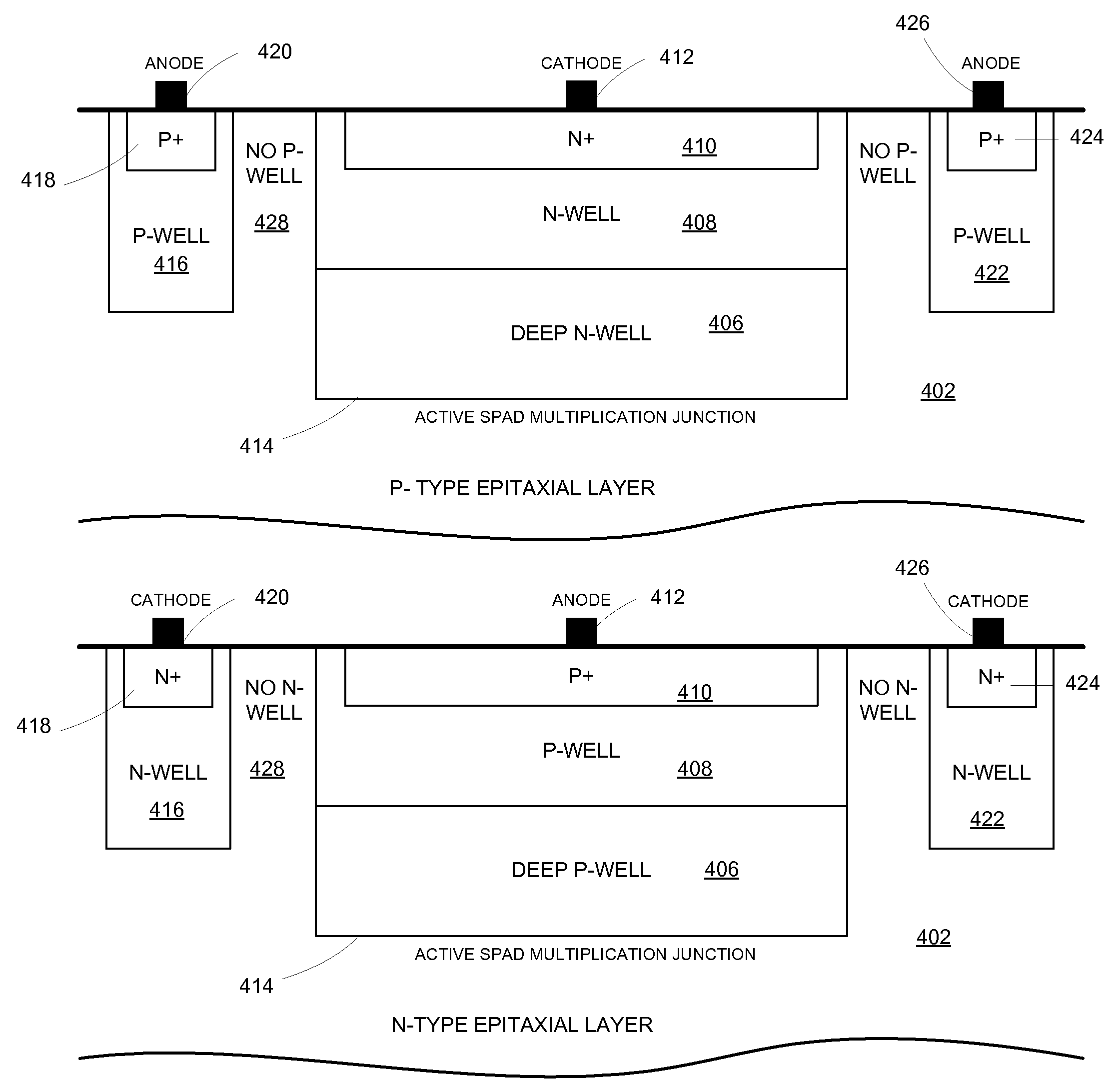
[0098]In the foregoing description, it will be appreciated that the examples given with regard to p-type and n-type materials can apply equally if the conductivity types are reversed (that is, n-type material is replaced by p-type and vice versa) with appropriate reversals of voltages, anodes / cathodes and the like. Portions of this document assume a p-type substrate as this is mostly standard in CMOS integrated circuits.

[0099]FIG. 4 is a schematic of a first embodiment of a single photon avalanche diode (SPAD) that is fabricated as part of a CMOS integrated circuit 400. The SPAD 404 is formed in the epitaxial layer (‘epi-layer’) 402 that has been grown on a substrate (not shown). A deep well 406 is implanted into the epi-layer 402 and covered with a well of the same conductivity type 408 that is connected in turn to a heavily doped electrode implant 410 which is connected to the contact 412. An implant of opposite conductivity type 416, 422 is formed around a guard ring 428, with a ...


PUM


Abstract

A single photon avalanche diode for use in a CMOS integrated circuit includes a deep n-well region formed above a p-type substrate and an n-well region formed above and in contact with the deep n-well region. A cathode contact is connected to the n-well region via a heavily doped n-type implant. A lightly doped region forms a guard ring around the n-well and deep n-well regions. A p-well region is adjacent to the lightly doped region. An anode contact is connected to the p-well region via a heavily doped p-type implant. The junction between the bottom of the deep n-well region and the substrate forms a multiplication region when an appropriate bias voltage is applied between the anode and cathode and the guard ring breakdown voltage is controlled with appropriate control of the lateral doping concentration gradient such that the breakdown voltage is higher than that of the multiplication region.

Description

PRIORITY CLAIM[0001]This application is a 371 filing of PCT / GB2011 / 051686 filed Sep. 8, 2011, which claims priority from Great Britain Application for Patent 1014843.5 filed Sep. 8, 2010, the disclosures of which are incorporated by reference.FIELD OF THE INVENTION[0002]The present invention relates to a single photon avalanche diode (SPAD) and a method of fabricating same, and relates in particular to SPADs manufactured in a CMOS fabrication process.BACKGROUND TO THE INVENTION[0003]Photodiodes convert light into electrical signals, and form the basis of a wide range of imaging and detection devices. Common configurations of photodiodes include PIN photodiodes, operated in photovoltaic or photoconductive mode, and single photon avalanche diodes (SPADs), typically operated in Geiger mode. Photodiodes can be realised using a number of different technologies, but it is particularly convenient and economical to form photodiodes using the CMOS fabrication process that has evolved as the ...

Claims


Application Information

Patent Timeline
Patent Type & Authority Patents(United States)
IPC IPC(8): H01L31/107H01L31/18H01L31/0232H01L31/0236H01L27/144
CPCH01L31/107H01L27/1443H01L31/02327H01L31/02363H01L31/18H01L31/1804Y02E10/547Y02P70/50
Inventor WEBSTER, ERIC ALEXANDER GARNERHENDERSON, ROBERT KERR
Owner STMICROELECTRONICS (RES & DEV) LTD
Why Eureka
Try Eureka