
Touchscreen panel sensor film and manufacturing method thereof

a technology of sensor film and touch screen, which is applied in the direction of electronic switching, pulse technique, instruments, etc., can solve the problems that the accuracy requirements are difficult to meet with any of the various manufacturing methods currently in use, and achieve the effects of reducing surface area, improving design quality, and enlarging the display region of the display devi

Active Publication Date: 2015-11-17
DAI NIPPON PRINTING CO LTD
View PDF69 Cites 3 Cited by
  • Summary
  • Abstract
  • Description
  • Claims
  • Application Information

AI Technical Summary

Benefits of technology

The present invention provides a highly reliable touchscreen panel sensor film that includes a small non-active area fabricated on a web or sheet. The sensor film is formed to improve both processing and interconnection accuracy between high-precision electrical lines and an FPC substrate, as well as position-matching accuracy with respect to a touchscreen panel device. The sensor film has accurate alignment marks or product information formed with a high degree of position accuracy in the same steps of those of the touchscreen panel sensor, without involving a new step. This simplifies the manufacturing process and improves the accuracy of the finished sensor film.

Problems solved by technology

These accuracy requirements, however, are difficult to satisfy with any of the various manufacturing methods currently in use, such as screen printing mentioned above.

Method used


Image

  • Touchscreen panel sensor film and manufacturing method thereof
  • Touchscreen panel sensor film and manufacturing method thereof
  • Touchscreen panel sensor film and manufacturing method thereof

Examples


first embodiment

[0176]Hereunder, a first embodiment of the present invention will be described referring to the accompanying drawings.

[0177]In the drawings attached to this specification, scales and dimensional aspect ratios are changed and exaggerated with respect to actual ones for convenience's sake of illustration and for better understanding of the invention.

[0178]The terms “sheet”, “film”, and “plate” that will appear herein are based only upon the differences in designation, and are not distinguished from one another. Therefore, the term “sheet”, for example, means a concept including such a member and portion as one may call a film, a plate, or the like.

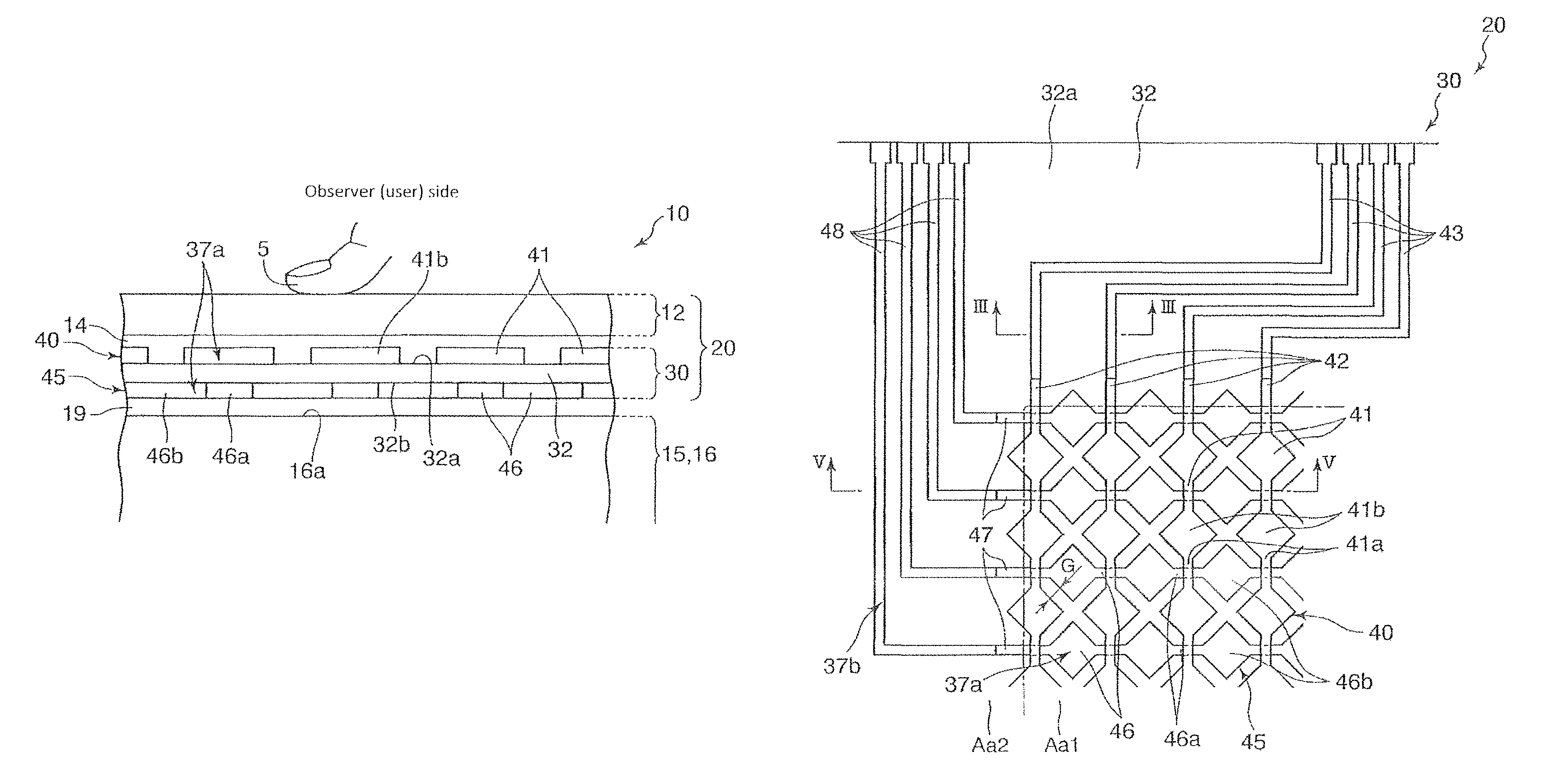
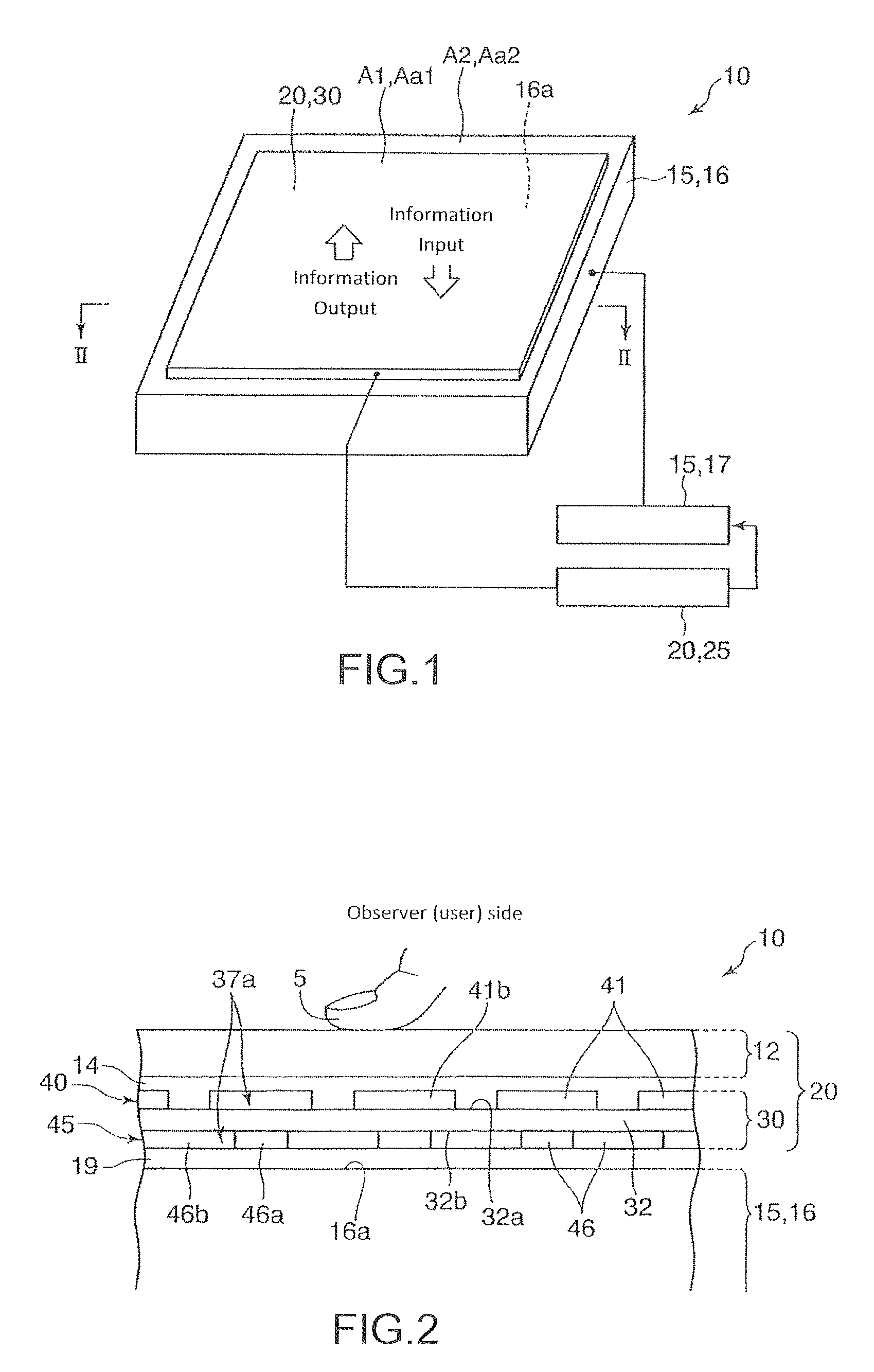
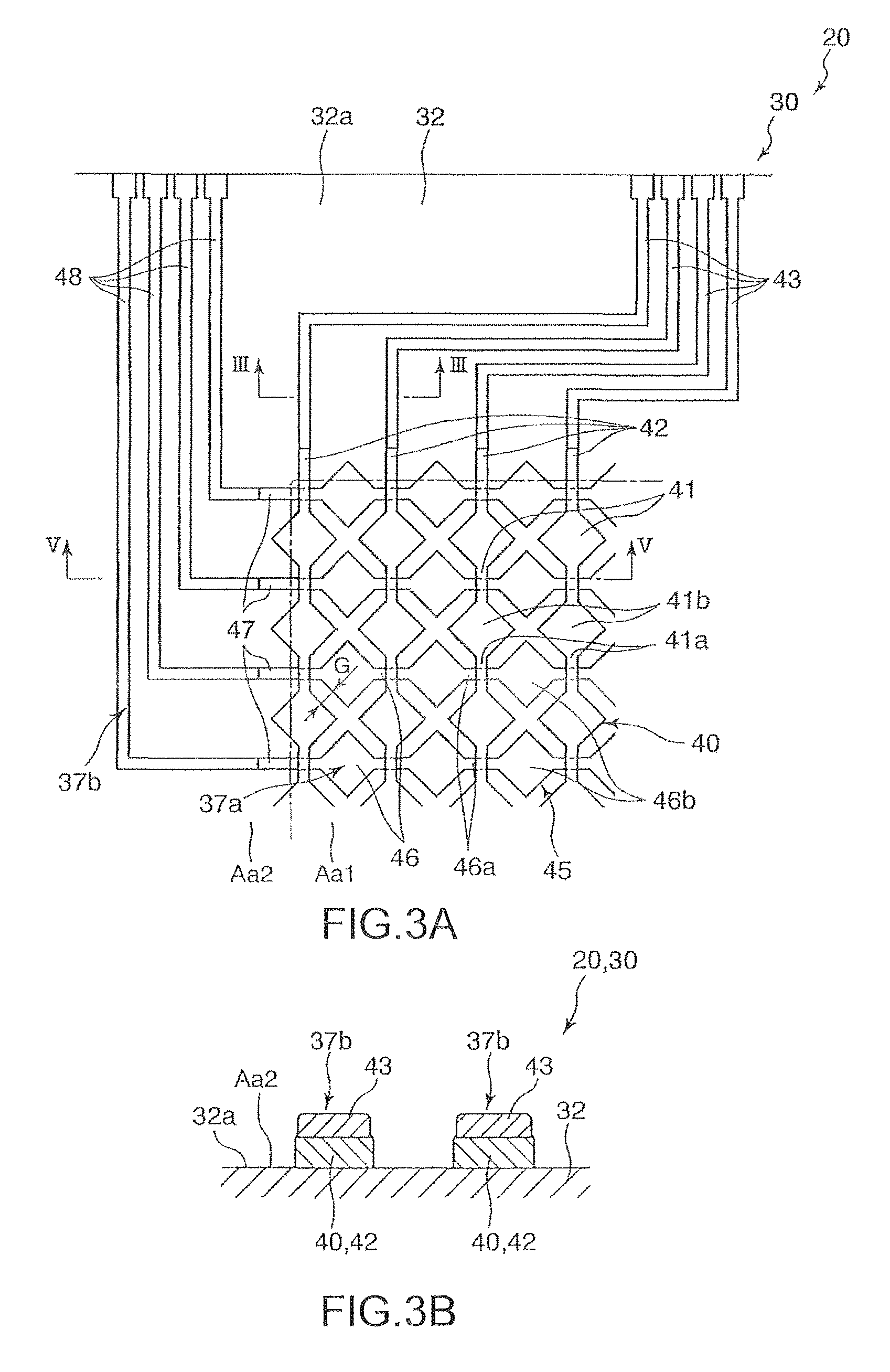
[0179]FIGS. 1 to 6 illustrate the first embodiment of the present invention. Of these figures, FIG. 1 is a diagram schematically showing a touchscreen panel device along with a display device, FIG. 2 is a sectional view showing a touchscreen panel sensor of the touchscreen panel device of FIG. 1 along with the display device, FIGS. 3A and 3B...

second embodiment

[0290]A second embodiment of the present invention is described below referring to FIGS. 12(a), 12(b) and 13. FIG. 12(a), which corresponds to FIG. 3B in the first embodiment, is a sectional view showing first electrical lead-out conductors provided in the second embodiment of the present invention, and FIG. 12(b) is a sectional view showing second electrical lead-out conductors provided in the second embodiment of the present invention. FIG. 13 is a sectional view showing a laminate provided in the second embodiment of the present invention.

[0291]The second embodiment shown in FIGS. 12(a), 12(b), and 13 differs from the first embodiment only in that: each lead-out conductor includes an intermediate layer provided on a portion of a transparent electrical conductor spacedly from a base film, and a highly conductive layer provided on the intermediate layer; the highly conductive layer is formed from a material whose conductivity is greater than that of materials forming the transparen...

third embodiment

[0317]Next, a third embodiment of the present invention is described below referring to FIGS. 18A to 20. The third embodiment shown in FIGS. 18A to 20 differs from the first and second embodiments only in that one pair of indexes are provided for evaluating the position accuracy of the patterns on one side of the touchscreen panel sensor and on the other side thereof, and all other configurational factors are substantially the same as those of the first and second embodiments. In the third embodiment of FIGS. 18A to 20, the same elements as used in the first and second embodiments are each assigned the same reference number, and further detailed description of these elements is omitted herein.

[0318]A shape and layer structure of the paired index portions are first described below referring to FIGS. 18A and 18B. FIG. 18A is a top view showing a touchscreen panel sensor piece 75 used in the present embodiment, and FIG. 18B is a sectional view of the touchscreen panel sensor piece 75.

[...


PUM

PropertyMeasurementUnit
photosensitiveaaaaaaaaaa

Abstract

Presented is a touchscreen panel sensor film with alignment marks or product information assigned thereto, this sensor film being formed so as to improve in post-processing accuracy. The touchscreen panel sensor film according to this invention includes a transparent base film and a transparent electrical conductor pattern provided on at least one surface of the base film, and achieves the improvement of post-processing accuracy by having alignment marks or product information in a non-active area on the sensor film.

Description

CROSS REFERENCE TO RELATED APPLICATIONS[0001]This application is a continuation of U.S. application Ser. No. 13 / 704,366, filed Mar. 6, 2013, which was the National Stage of International Application No. PCT / JP2011 / 070525, filed Sep. 8, 2011, and claims the benefit under 35 USC §119(a)-(d) of Japanese Patent Application Nos. 2010-219774, filed Sep. 29, 2010, and 2011-141603, filed on Jun. 27, 2011, the entireties of which are incorporated herein by reference. The entire disclosure of Japanese Patent Application Nos. 2009-86477, filed Mar. 31, 2009, and 2009-273798, filed Dec. 1, 2009, are also incorporated herein by reference.FIELD OF THE INVENTION[0002]The present invention relates to touchscreen panel sensor films and manufacturing methods thereof.BACKGROUND OF THE INVENTION[0003]Nowadays, touchscreen panel devices are widely used as input means. The touchscreen panel devices include a touchscreen panel sensor, a control circuit for detecting a contact position of an object on the ...

Claims


Application Information

Patent Timeline
Patent Type & Authority Patents(United States)
IPC IPC(8): G06F1/16H03K17/96G06F3/044G06F3/045G02F1/1333
CPCG06F1/1692G02F1/13338G06F3/044G06F3/045H03K17/9622G06F2203/04103G06F2203/04112G06F3/0445G06F3/0446
Inventor TAKAHASHI, MASAHIROIIDA, MITSURUMATSUMOTO, YUTAKAMATSUDA, JUNZOOGAWA, KAZUYAISHIGAMI, TATSUHIKO
Owner DAI NIPPON PRINTING CO LTD
Learn More