Liquid crystal display panel and its manufacturing method

a technology of liquid crystal display and manufacturing method, which is applied in the direction of non-linear optics, instruments, optics, etc., can solve the problems of discontinuous formation of sealants, disconnection of sealants, and non-uniform width of sealants, so as to reduce the reduction of end face strength in an lcd panel and reduce the effect of end face strength

Inactive Publication Date: 2011-11-17
SHARP KK
View PDF9 Cites 3 Cited by
  • Summary
  • Abstract
  • Description
  • Claims
  • Application Information

AI Technical Summary

Benefits of technology

[0035]According to the present invention, a sealant for bonding a first substrate and a second substrate has a first seal portion and a second seal portion having a smaller width than the first seal portion, and the second substrate is thinner than the first substrate. Thus, reduction in end face strength in an LCD panel can be suppressed, whereby the outer dimensions thereof are stabilized. Moreover, a display region can be increased.

Problems solved by technology

Thus, the nozzle can get clogged while drawing the sealant, which causes not only a non-uniform width of the sealant, but also disconnections of the sealant, that is, discontinuous formation of the sealant.
Moreover, when the sealant is formed by a seal printing method using a screen printing plate, clogging of the screen printing plate can result in a non-uniform width of the sealant and disconnections of the sealant, as in the case of the dispense method.
If the glass substrates have a sealant in a region to which the low-temperature liquid material is to be injected, or in a cutting region such as a region where the scribe line is to be formed, the sealant tends to induce unintended breakage and cracks of the glass substrates, thereby causing defective cutting.
Thus, it is difficult to form a thin sealant in view of the uniformity of the sealant width and the disconnections of the sealant as described above.

Method used


Image

  • Liquid crystal display panel and its manufacturing method
  • Liquid crystal display panel and its manufacturing method
  • Liquid crystal display panel and its manufacturing method

Examples


Embodiment Construction

[0062]Hereinafter, an embodiment of the present invention will be described in detail based on the accompanying drawings. Note that the present invention is not limited to the following embodiment.

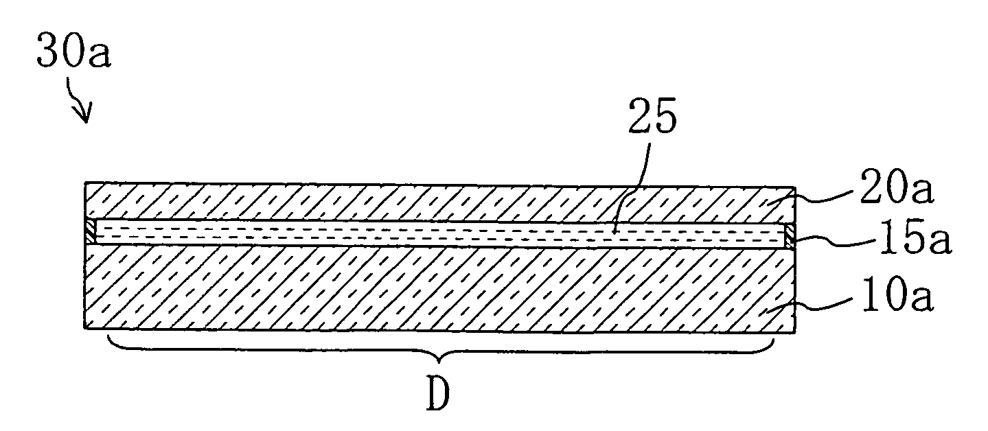
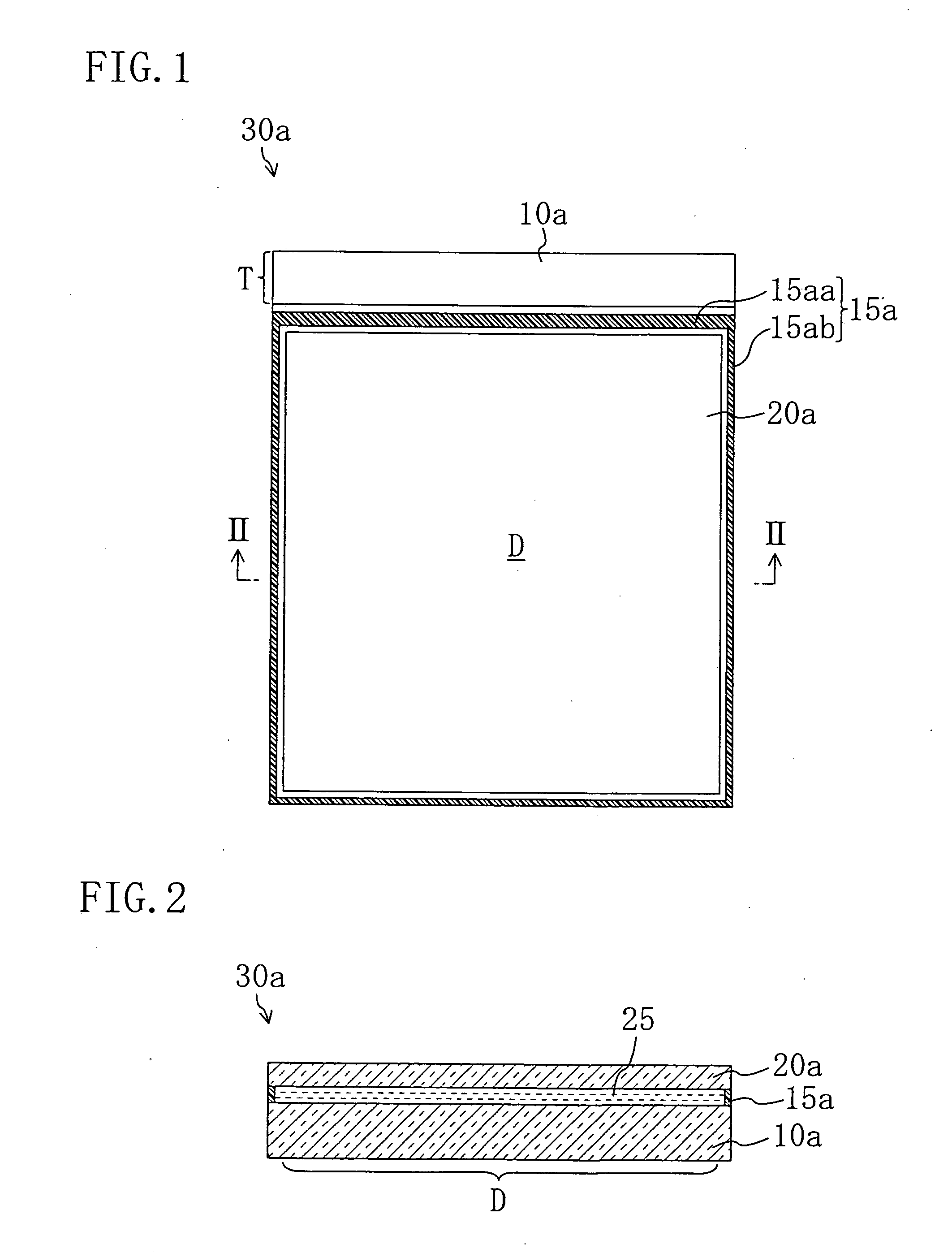
[0063]FIG. 1 is a plan view of an LCD panel 30a of the present embodiment, and FIG. 2 is a cross-sectional view of the LCD panel 30a taken along line II-II in FIG. 1.

[0064]As shown in FIGS. 1 and 2, the LCD panel 30a includes a TFT substrate (first substrate) 10a and a CF substrate (second substrate) 20a which are positioned so as to face each other, a liquid crystal layer 25 provided between the TFT substrate 10a and the CF substrate 20a, and a sealant 15a formed in a rectangular frame shape for bonding the TFT substrate 10a and the CF substrate 20a to each other, and enclosing the liquid crystal layer 25 therebetween.

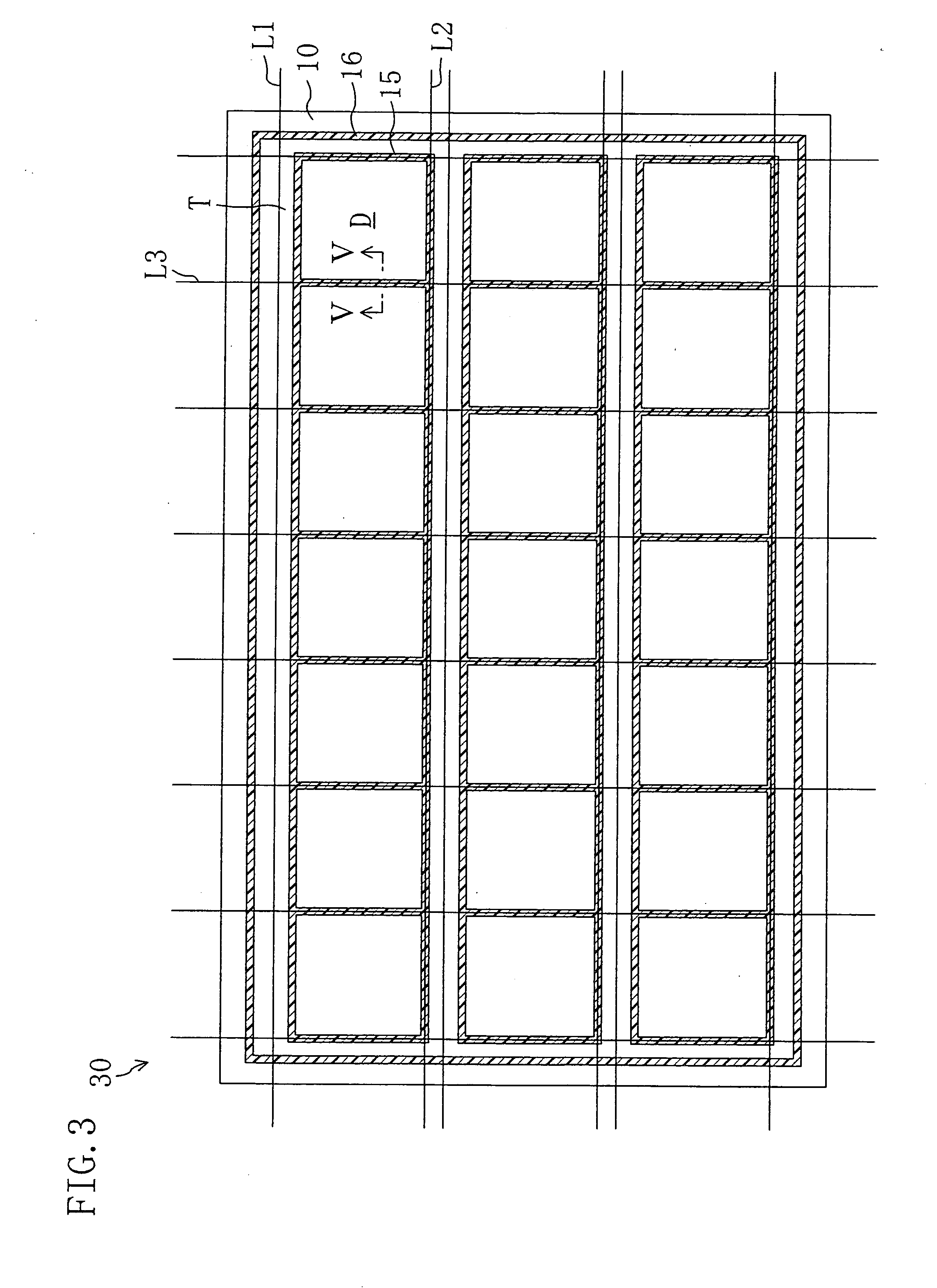
[0065]The TFT substrate 10a includes a plurality of gate lines (not shown) extending parallel to each other on a glass substrate, a plurality of source lines (not shown) ext...


PUM

PropertyMeasurementUnit
thicknessaaaaaaaaaa
thicknessaaaaaaaaaa
widthaaaaaaaaaa

Abstract

A liquid crystal display panel includes: a first substrate 10a made of glass; a second substrate 20a which is made of glass, is located so as to face the first substrate 10a, and has a smaller thickness than that of the first substrate 10a; a liquid crystal layer 25 provided between the first substrate 10a and the second substrate 20a; and a frame-shaped sealant 15a for bonding the first substrate 10a and the second substrate 20a to each other, and enclosing the liquid crystal layer 25 therebetween. The sealant 15a includes a first seal portion 15aa provided along a side where one of the first substrate 10a and the second substrate 20a protrudes with respect to the other, and a second seal portion 15ab which is provided along a side where respective end faces of the first substrate 10a and the second substrate 20a are aligned with each other, and which is provided so that an end face of the second seal portion 15ab is aligned with the substrate end faces, and so that the second seal portion 15ab has a smaller width than that of the first seal portion 15aa.

Description

TECHNICAL FIELD[0001]The present invention generally relates to a liquid crystal display (LCD) panel and a manufacturing method thereof. More particularly, the present invention relates to a technique of cutting a glass substrate of an LCD panel.BACKGROUND ART[0002]In recent years, there has been a growing demand for reduction in thickness and weight of a panel main body for improved portability, and for increase in display region with respect to outside dimensions of a panel, in LCD panels for use in mobile equipment applications such as cellular phones, portable digital assistants, and portable games.[0003]As for reduction in thickness and weight, glass substrates for fabricating a TFT (Thin Film Transistor) substrate and a CF (Color Filter) substrate of an LCD panel have been reduced in thickness recently. More specifically, the panel thickness was conventionally 1.0 mm or more by combinations of a 0.7 mm-thick TFT substrate and a 0.7 mm-thick CF substrate, a 0.5 mm-thick TFT sub...

Claims


Application Information

Patent Timeline
Patent Type & Authority Applications(United States)
IPC IPC(8): G02F1/1339
CPCG02F1/1339G02F1/133351
Inventor YAMAGISHI, SHINJI
Owner SHARP KK
Why Eureka
Try Eureka