

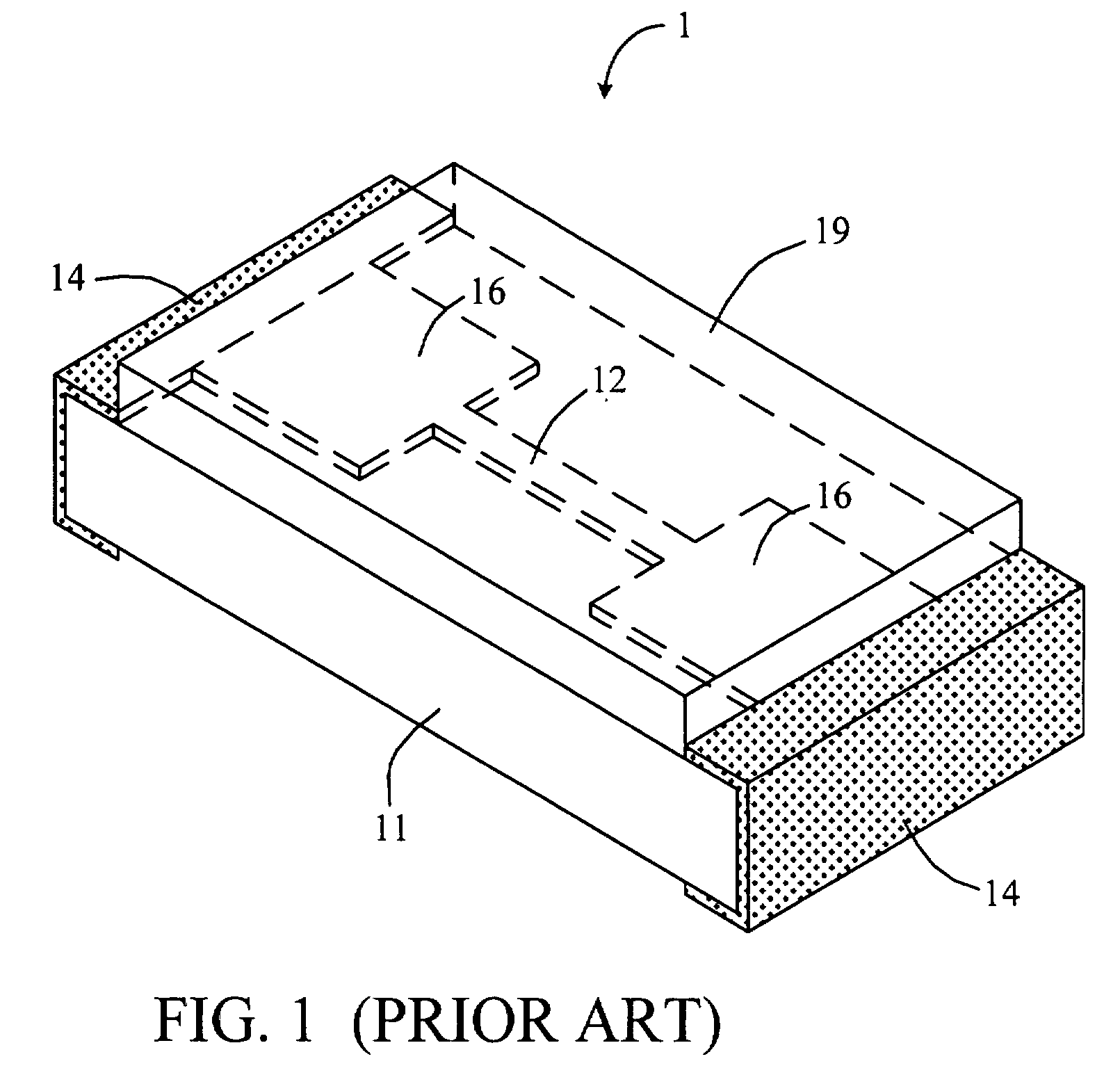
Chip-type fuse and method of manufacturing the same
a technology of chip-type fuse and manufacturing method, which is applied in the direction of basic electric elements, emergency protective devices, electrical equipment, etc., can solve the problems of fire disaster, too large traditional fuse size to meet the miniaturization requirement of current electronic products, and arc is a kind of rapid and localized high energy
- Summary
- Abstract
- Description
- Claims
- Application Information
AI Technical Summary
Benefits of technology
Problems solved by technology
Method used
Image

Examples
Embodiment Construction
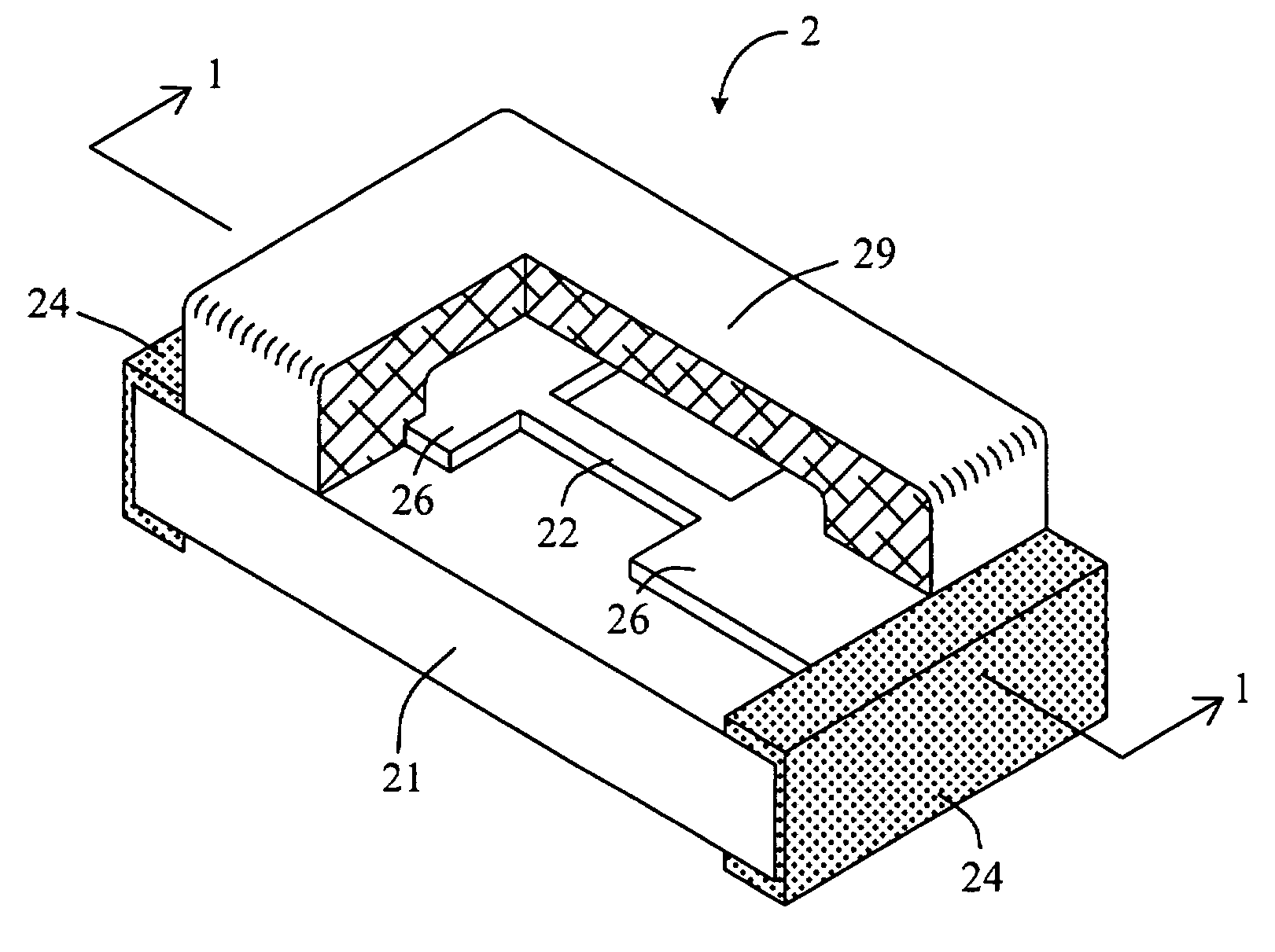
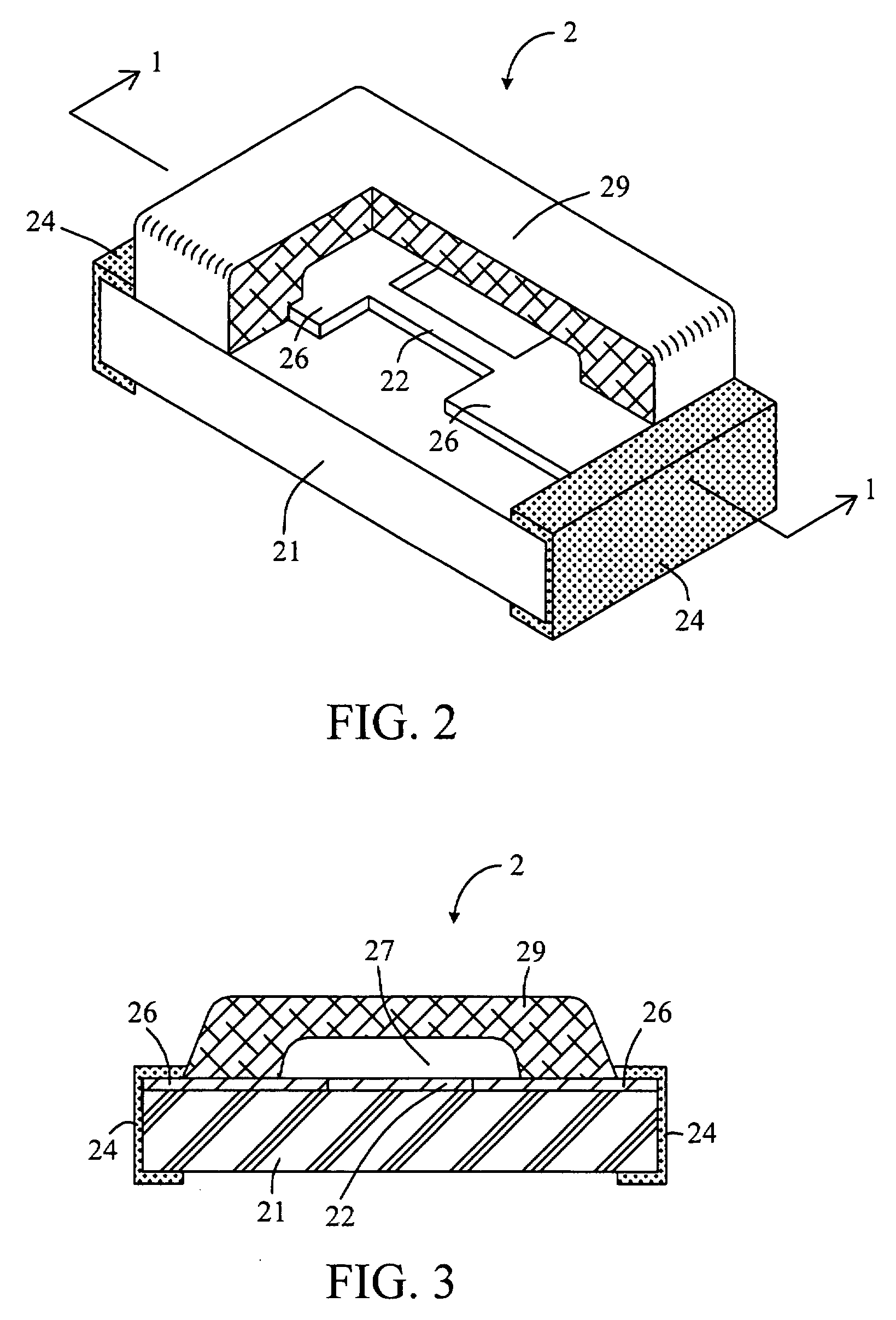
[0027]Referring to FIG. 2, a perspective view of chip-type fuse 2 according to a preferred embodiment of the invention is depicted. The protective layer 29 is partially removed to reveal the internal structure. FIG. 3 is a cross-sectional view of FIG. 2 along the centerline of width (1-1 line). Chip-type fuse 2 comprises a substrate 21, a fusible element 22, a cavity 27, a protective layer 29, two terminals 24, and two termination pads 26.
[0028]The substrate 21 is made of alumina of more than 90% purity, glass, or other electrically insulating ceramics. Alumina of 96% purity is very popular with a thickness of 0.2 to 1.0 mm.
[0029]The fusible element 22 is an electrically conductive film disposed over the surface of substrate 21. The fusible element 22 consists of pure metal or alloy including gold, silver, aluminum, copper, platinum, etc., or a composite of silver and glass. The two ends of fusible element 22 are electrically connected with the two conductive termination pads 26 res...
PUM
| Property | Measurement | Unit |
|---|---|---|
| pressure | aaaaa | aaaaa |
| thickness | aaaaa | aaaaa |
| width | aaaaa | aaaaa |
Abstract
Description
Claims
Application Information