Phase change memory devices with contact surface area to a phase changeable material defined by a sidewall of an electrode hole and methods of forming the same

Active Publication Date: 2005-05-26
SAMSUNG ELECTRONICS CO LTD
View PDF4 Cites 78 Cited by
  • Summary
  • Abstract
  • Description
  • Claims
  • Application Information

AI Technical Summary

Benefits of technology

[0020] Patterning the insulation layer to form a guide hole and forming an electrode hole may include patterning the insulation layer to form the guide hole to expose a region of the heating electrode corresponding to the electrode hole and selectively etching the exposed region of the heating electrode to form the electrode hole. Patterning the insulation layer to form a guide hole may include patterning the insulation layer to form a guide hole having an inclined sidewall where a bottom end width of the guide hole is smaller than a top end width of the guide hole. Patterning the insulation layer to form a guide hole having an inclined sidewall and forming an electrode hole may include applying a patterning process including a slope-etch process to the insulation layer to form the guide hole exposing a region of the heating electrode corresponding to the electrode hole and having an inclined sidewall and selectively etching the exposed region of the heating electrode to form the electrode hole. P

Problems solved by technology

Furthermore, fabrication of conventional flash memory devices may be complicated.
In addition, pow

Method used


Image

  • Phase change memory devices with contact surface area to a phase changeable material defined by a sidewall of an electrode hole and methods of forming the same
  • Phase change memory devices with contact surface area to a phase changeable material defined by a sidewall of an electrode hole and methods of forming the same
  • Phase change memory devices with contact surface area to a phase changeable material defined by a sidewall of an electrode hole and methods of forming the same

Examples


Example

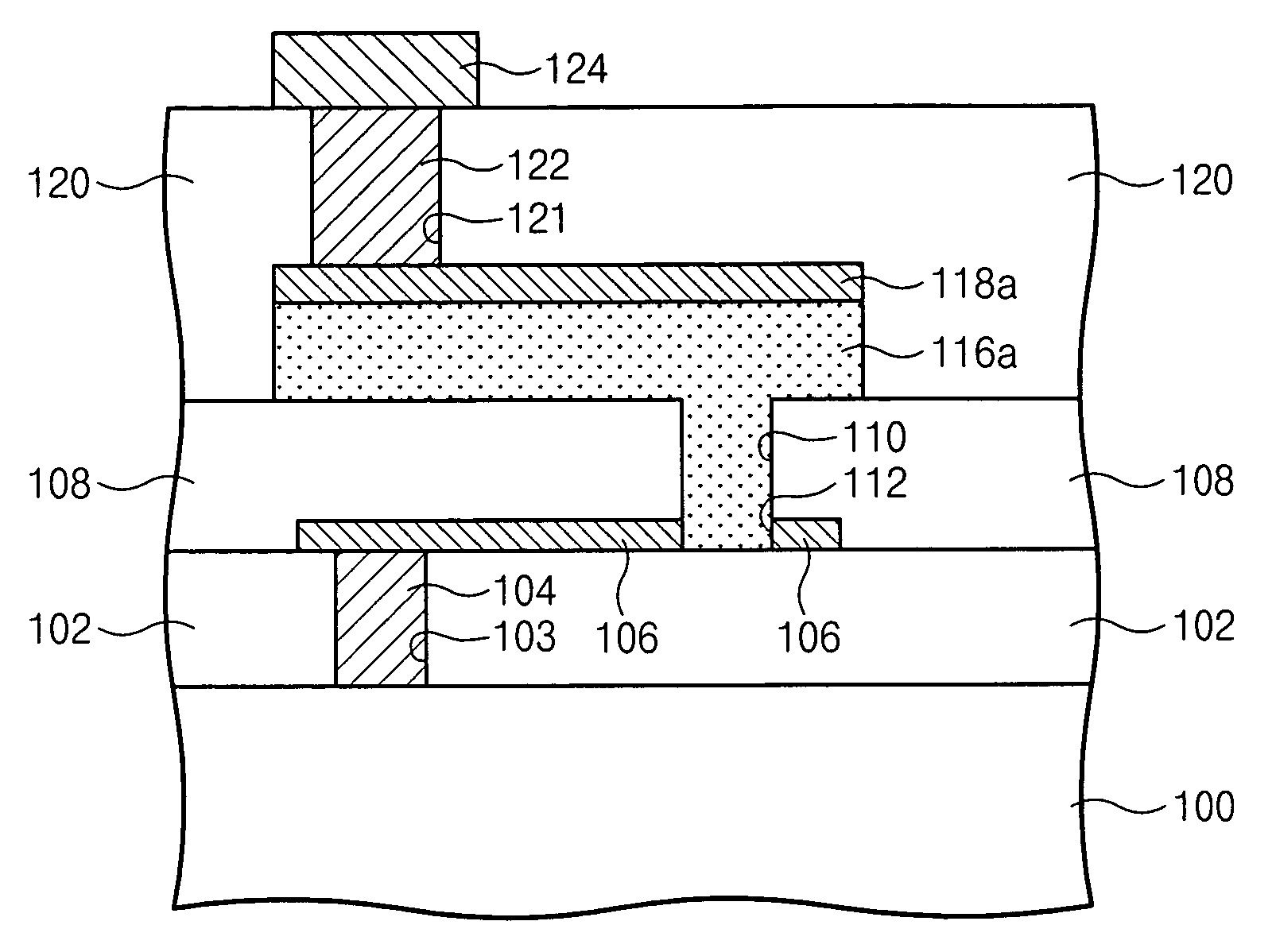
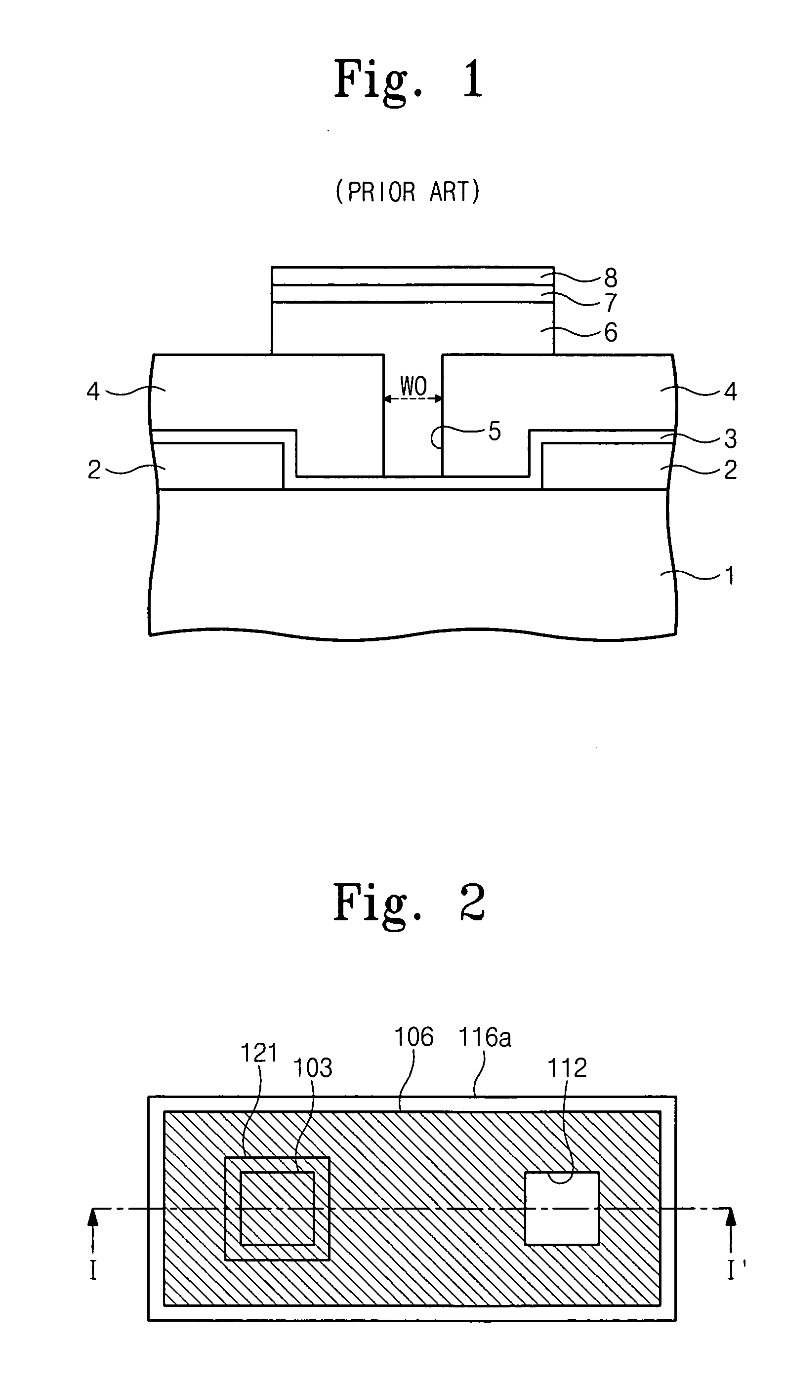
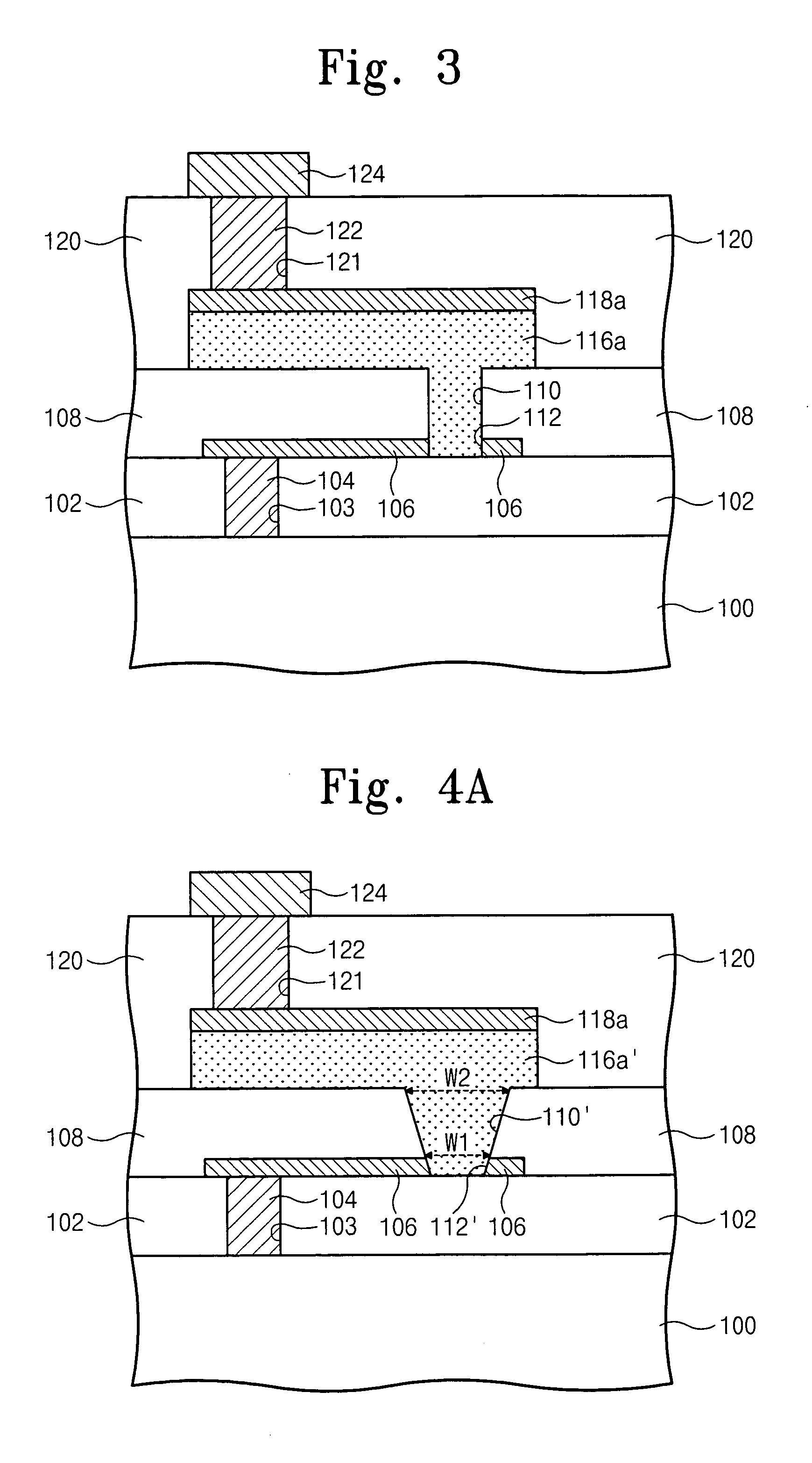
[0033] The present invention now will be described more fully hereinafter with reference to the accompanying drawings, in which embodiments of the invention are shown. However, this invention should not be construed as limited to the embodiments set forth herein. Rather, these embodiments are provided so that this disclosure will be thorough and complete, and will fully convey the scope of the invention to those skilled in the art. In the drawings, the thickness of layers and regions are exaggerated for clarity. Like numbers refer to like elements throughout. As used herein the term “and / or” includes any and all combinations of one or more of the associated listed items.

[0034] It will be understood that when an element such as a layer, region or substrate is referred to as being “on” or extending “onto” another element, it can be directly on or extend directly onto the other element or intervening elements may also be present. In contrast, when an element is referred to as being “d...


PUM


Abstract

Phase change memory devices and methods of making phase changeable memory devices including a heating electrode disposed on a substrate are provided. The heating electrode includes an electrode hole in the heating electrode. A phase change material pattern is provided in the electrode hole and contacts a sidewall of the electrode hole. In some embodiments, the electrode hole extends through the heating electrode. In some embodiments, the phase changeable material pattern only contacts the electrode at a sidewall of the electrode hole

Description

CLAIM OF PRIORITY [0001] This application claims priority from Korean Patent Application No. 2003-083551, filed on Nov. 24, 2003, in the Korean Intellectual Property Office, the contents of which are hereby incorporated by reference in their entirety as if set forth fully herein. FIELD OF THE INVENTION [0002] The present invention relates to semiconductor devices and methods of forming the same and, more particularly, to phase change memory devices and methods of forming the same. BACKGROUND OF THE INVENTION [0003] In non-volatile memory devices, unit cells of the device maintain data stored in the unit cells even when a power supply is cut off. Widely used non-volatile memory devices include flash memory devices. Unit cells of conventional flash memory devices, typically, have an electrically insulated floating gate. Depending on whether the electrons in the floating gate exist or not (or a variation of an amount of the electrons), the data stored in the flash memory cell may be de...

Claims


Application Information

Patent Timeline
IPC IPC(8): G01C1/10H01L27/105G11C11/56G11C13/00H01L27/10H01L27/108H01L45/00
CPCH01L45/1666H01L45/122H01L45/144H01L45/126H01L45/143H01L45/06H10N70/821H10N70/8413H10N70/231H10N70/8825H10N70/061H10N70/8828H10B12/00
Inventor JEONG, WON-CHEOLKIM, HYEONG-JUNPARK, JAE-HYUNJEONG, CHANG-WOOK
Owner SAMSUNG ELECTRONICS CO LTD
Why Eureka
Try Eureka