Multi-BIOS circuit and switching method between multiple BIOS chips

a bios circuit and switching method technology, applied in the field of computers and storage, can solve the problems of unstable work environment, inability to power on or start the computer, increase the maintenance cost and time, degrade the user experience in use, etc., and achieve the effect of low risk, high safety and reliability, and convenient operation

Active Publication Date: 2015-12-08
CELESTICA TECH CONSULTANCY SHANGHAI
View PDF3 Cites 2 Cited by
  • Summary
  • Abstract
  • Description
  • Claims
  • Application Information

AI Technical Summary

Benefits of technology

[0007]An objective of the present invention is to provide a circuit and a method which can conveniently accomplish starting by switching between multiple BIOSs and feature a low risk and high safety and reliability.
[0017]A further objective of the subject application is to provide a method of starting by switching between multiple BIOS chips in a multi-BIOS circuit. The multi-BIOS circuit comprises at least two BIOS chips, and an SPI Select chip is disposed between the BIOS chips and a Southbridge chip and electrically connected with the Southbridge chip and the BIOS chips via pins respectively so that starting by switching between the multiple BIOS chips can be accomplished.
[0040]The multi-BIOS circuit of the present invention significantly enhances the safety of computers, and features a higher stability and simple operations such as the BIOS starting and content copying so that a common user can operate the multi-BIOS circuit without instructions of a professional.

Problems solved by technology

Some storage or server products often require apparatuses to have a higher stability, accordingly, a plurality of BIOSs are disposed on a motherboard to prevent loss or damage of motherboard BIOS parameters when one or some of the BIOSs upgraded is failed or when one of some of the BIOSs are damaged by CIH viruses or the like, which would lead to phenomena such as that the computers cannot be powered on or started or the work environment is unstable.
When the aforesaid problems occur, common computer users, except professional maintenance personnel and technicians, may be unable to solve these problems by themselves, and this increases the maintenance cost and time and degrades the users' experience in use.
However, if a plurality of BIOSs are disposed on a motherboard, even one of the BIOSs is damaged, the system can still be started from other undamaged BIOSs so that there will be no loss.
The aforesaid ways have the following drawbacks: firstly, the safety is low especially for the first way, and the dual-BIOS system will break down once the BIOS chip is physically damaged; and secondly, the jumper setting of pin needs to be performed by opening the housing and is relatively complex, so it is inconvenient for the common users to perform this operation and other hardware apparatuses may even be damaged when the housing is opened.
It utilizes the switching function of switch elements to enable the system to be started from two BIOS chips provided with different program codes, and the way in this such application still lacks intelligence and convenience and adds to the complexity in use.
The operating way in this application is still complex and lacks intelligence and initiative.

Method used


Image

  • Multi-BIOS circuit and switching method between multiple BIOS chips
  • Multi-BIOS circuit and switching method between multiple BIOS chips

Examples


embodiment 1

[0059 Circuit Comprising Two BIOSs

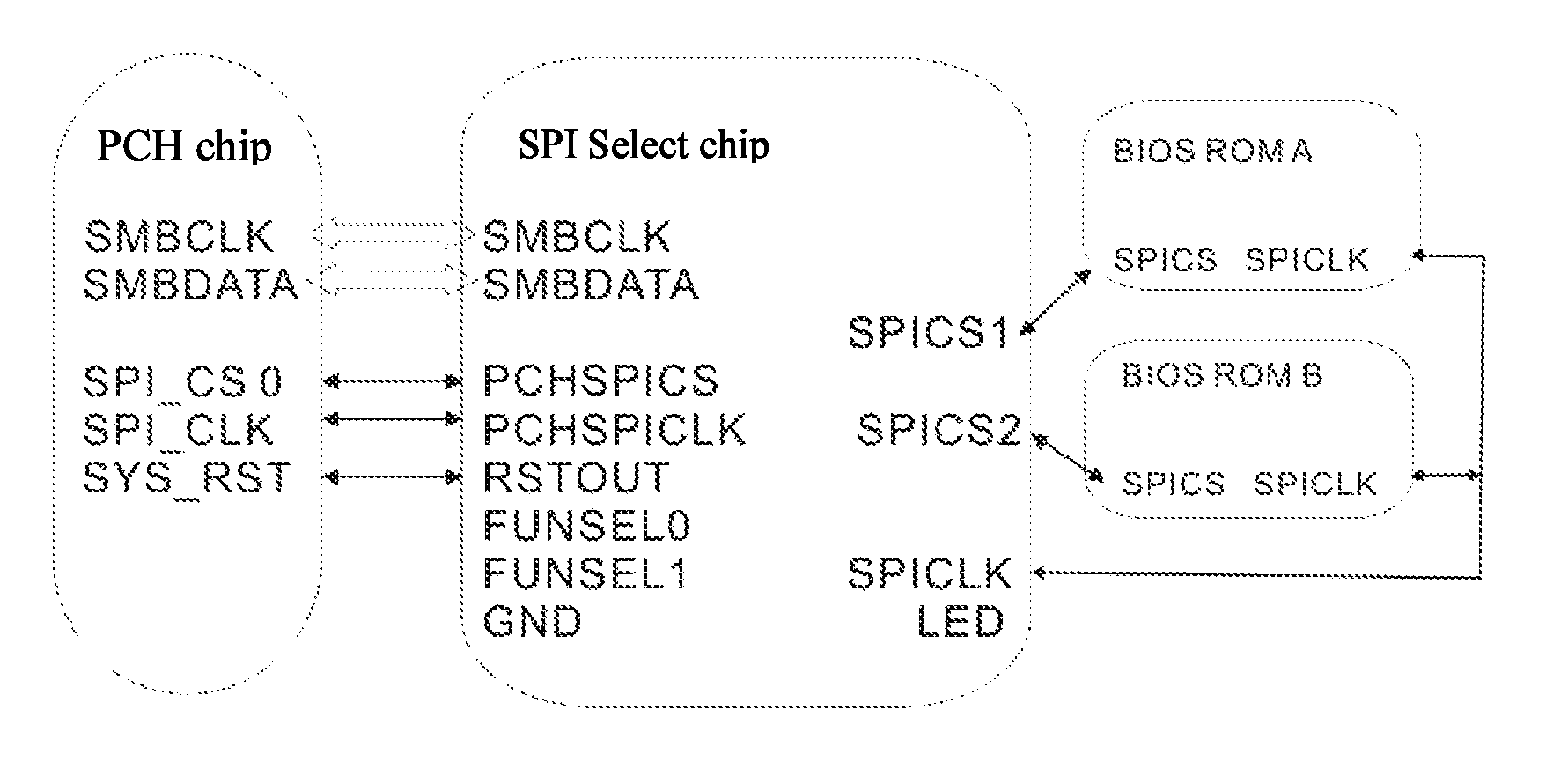
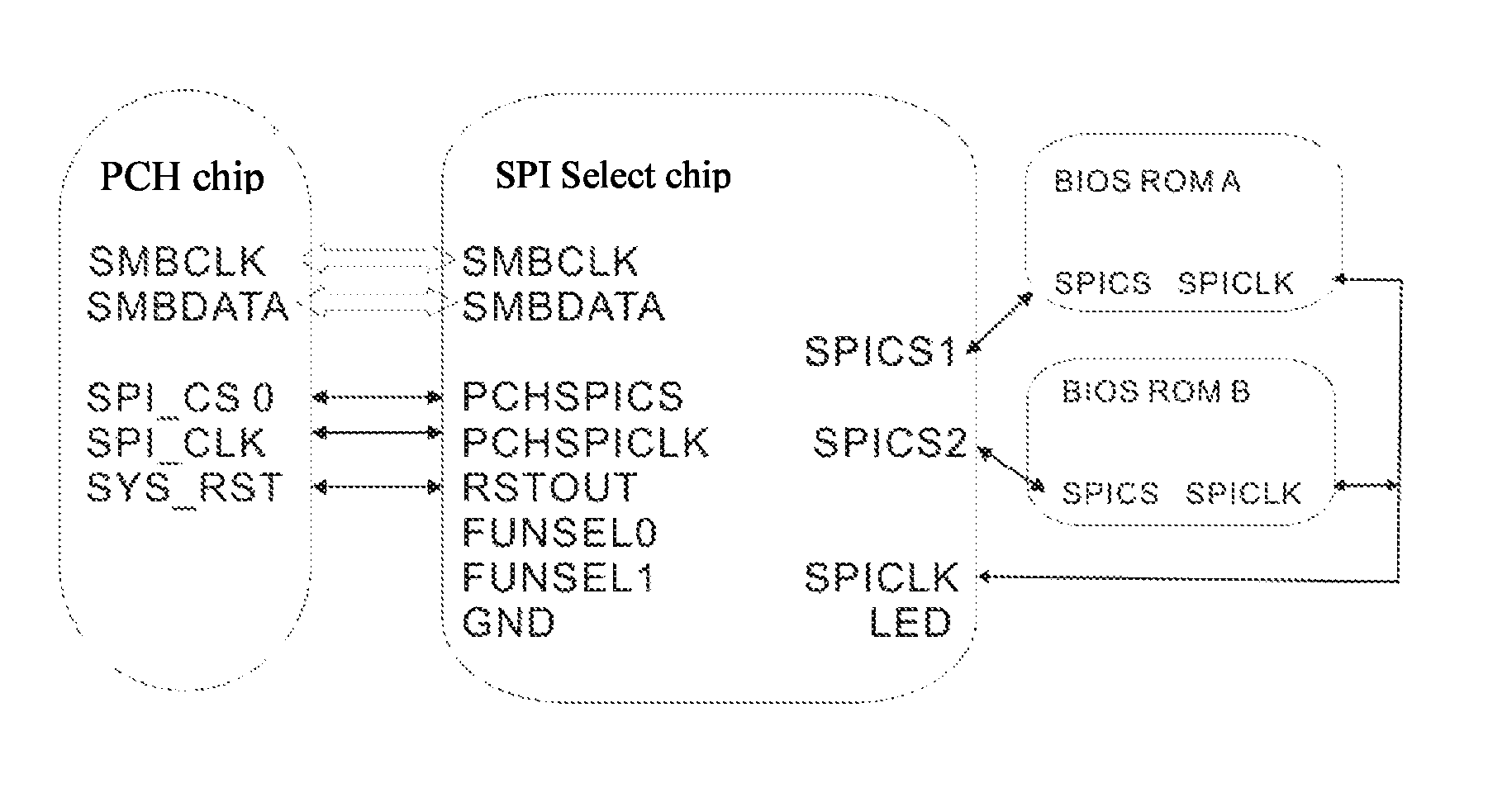
[0060]The circuit of the computer motherboard is provided with two BIOS chips (i.e., a BIOS A chip and a BIOS B chip) therein. An SPICS pin of the BIOS A chip is connected with an SPICS1 pin of the SPI Select chip, and an SPICLK pin of the BIOS A chip is connected with a SPICLK pin of the SPI Select chip. An SPICS pin of the BIOS B chip is connected with an SPICS2 pin of the SPI Select chip, and an SPICLK pin of the BIOS B chip is connected with the SPICLK pin of the SPI Select chip. An SMBCLK pin and a SMBDATA pin of the SPI Select chip are connected to an SMBCLK pin and an SMBDATA pin of a Southbridge chip through two SMBus lines respectively, a PCHSPICS pin of the SPI Select chip is connected to an SPI_CS0 pin of the Southbridge chip, a PCHSPICLK pin is connected to an SPI_CLK pin of a PCH chip, and an RSTOUT output pin of the SPI Select chip is connected to an SYS_RST pin of the PCH chip.

[0061](I) Selection of the BIOS Chips During Startup[0062]...

embodiment 2

[0072 Circuit Comprising three BIOSs

[0073]The circuit of the computer motherboard is provided with three BIOS chips (i.e., a BIOS A chip, a BIOS B chip and a BIOS C chip) therein. An SPICS pin of the BIOS A chip is connected with an SPICS1 pin of the SPI Select chip, and an SPICLK pin of the BIOS A chip is connected with an SPICLK pin of the SPI Select chip. An SPICS pin of the BIOS B chip is connected with an SPICS2 pin of the SPI Select chip, and an SPICLK pin of the BIOS B chip is connected with the SPICLK pin of the SPI Select chip. An SPICS pin of the BIOS C chip is connected with an SPICS3 pin of the SPI Select chip, and an SPICLK pin of the BIOS C chip is connected with the SPICLK pin of the SPI Select chip. An SMBCLK pin and an SMBDATA pin of the SPI Select chip are connected to an SMBCLK pin and a SMBDATA pin of a Southbridge chip through two SMBus lines respectively, a PCHSPICS pin of the SPI Select chip is connected to an SPI_CS0 pin of the Southbridge chip, a PCHSPICLK p...


PUM


Abstract

The present invention relates to a multi-BIOS circuit and a BIOS switching method accomplished through the circuit. The multi-BIOS circuit comprises at least two BIOS chips, a SPI Select chip is disposed between the BIOS chips and a Southbridge chip, the BIOS chips are connected to the SPI Select chip pins, and the SPI Select chip is connected to the Southbridge chip pins. The present invention can significantly enhance the safety of computers, and increases the stability as well as the convenience in use and operation.

Description

[0001]This application claims priority to Chinese Patent Application No. 201210143810.3 filed on May 10, 2012.BACKGROUND OF THE INVENTION[0002]The subject application generally relates to computers, storage in computers or servers. More particularly, the subject application relates to a circuit including multiple BIOS chips and to a switch circuit between multiple BIOS chips and a method of multi-BIOS switching.[0003]Some storage or server products often require apparatuses to have a higher stability, accordingly, a plurality of BIOSs are disposed on a motherboard to prevent loss or damage of motherboard BIOS parameters when one or some of the BIOSs upgraded is failed or when one of some of the BIOSs are damaged by CIH viruses or the like, which would lead to phenomena such as that the computers cannot be powered on or started or the work environment is unstable. When the aforesaid problems occur, common computer users, except professional maintenance personnel and technicians, may ...

Claims


Application Information

Patent Timeline
Patent Type & Authority Patents(United States)
IPC IPC(8): G06F9/44G06F11/14G06F11/32
CPCG06F9/4401G06F11/1417G06F11/325
Inventor JIANG, JIAPINGWANG, JINBAO
Owner CELESTICA TECH CONSULTANCY SHANGHAI
Why Eureka
Try Eureka