

Light-emitting element with multiple light-emitting layers having controlled carrier mobility and lighting device and electronic device using the same
a light-emitting element and carrier technology, applied in the field of light-emitting elements and light-emitting devices, can solve the problems of reducing the reliability of light-emitting elements, reducing the emission efficiency, and reducing the efficiency of emission, so as to achieve high emission efficiency and reliable effect, the luminance is not easily decreased during operation
- Summary
- Abstract
- Description
- Claims
- Application Information
AI Technical Summary
Benefits of technology
Problems solved by technology
Method used
Image

Examples
embodiment 1
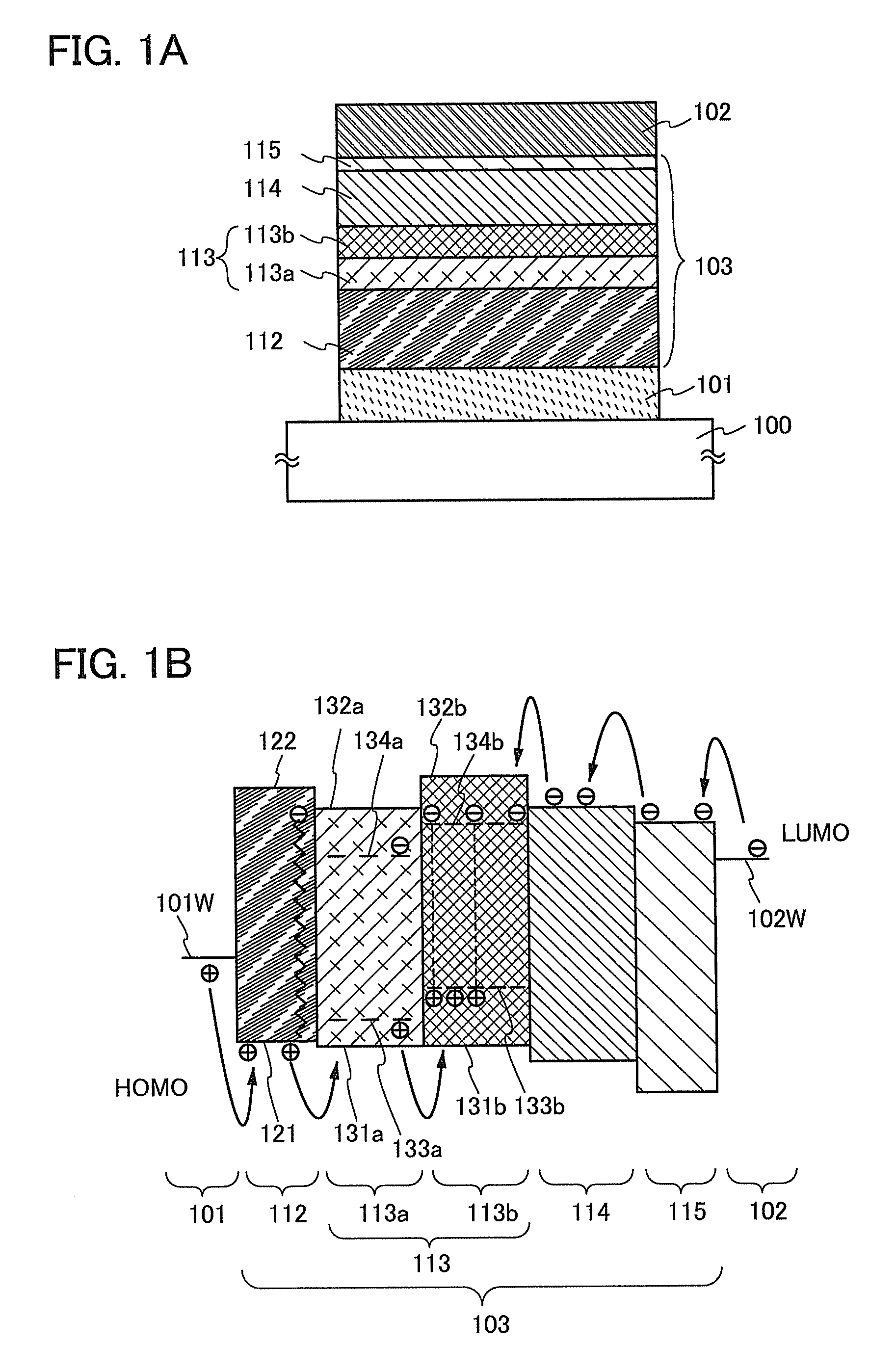
[0065]A light-emitting element which is described in this embodiment includes at least a first light-emitting layer whose one side is in contact with a hole-transport layer and a second light-emitting layer which is in contact with the other side of the first light-emitting layer. Both the first light-emitting layer and the second light-emitting layer contain a bipolar host material and a guest material which is a light-emitting material. The guest material contained in the first light-emitting layer has a lower ability for capturing a hole than the guest material contained in the second light-emitting layer; therefore, the hole-transport property of the first light-emitting layer is higher than that of the second light-emitting layer. As a result, holes are transported into a region apart from the hole-transport layer, and a recombination region of holes and electrons are formed widely in the light-emitting layers. Furthermore, an anti-reducing material is contained in the hole-tra...
embodiment 2
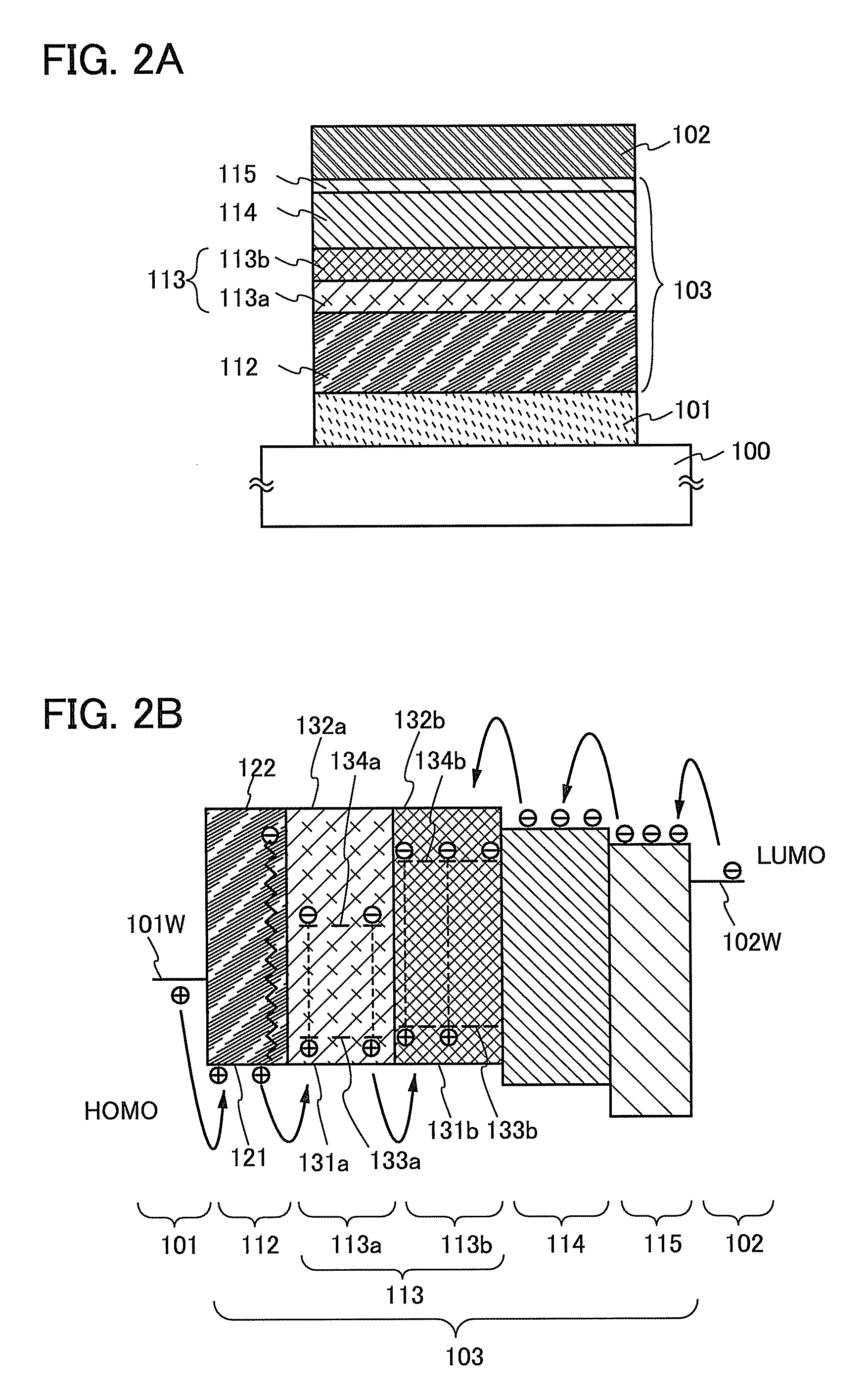
[0147]A light-emitting element illustrated in this embodiment includes at least a first light-emitting layer whose one side is in contact with a hole-transport layer, and a second light-emitting layer in contact with the other side of the first light-emitting layer. Both the first light-emitting layer and the second light-emitting layer contain a bipolar host material and a guest material which is a light-emitting material. The guest material contained in the first light-emitting layer has a low ability for capturing a hole than the guest material contained in the second light-emitting layer; therefore, the hole-transport property of the first light-emitting layer is higher than that of the second light-emitting layer. As a result, holes are transported to a region apart from the hole-transport layer, and a recombination region of holes and electrons is formed widely in the light-emitting layers. Emission colors of the light-emitting material contained in the first light-emitting la...
embodiment 3
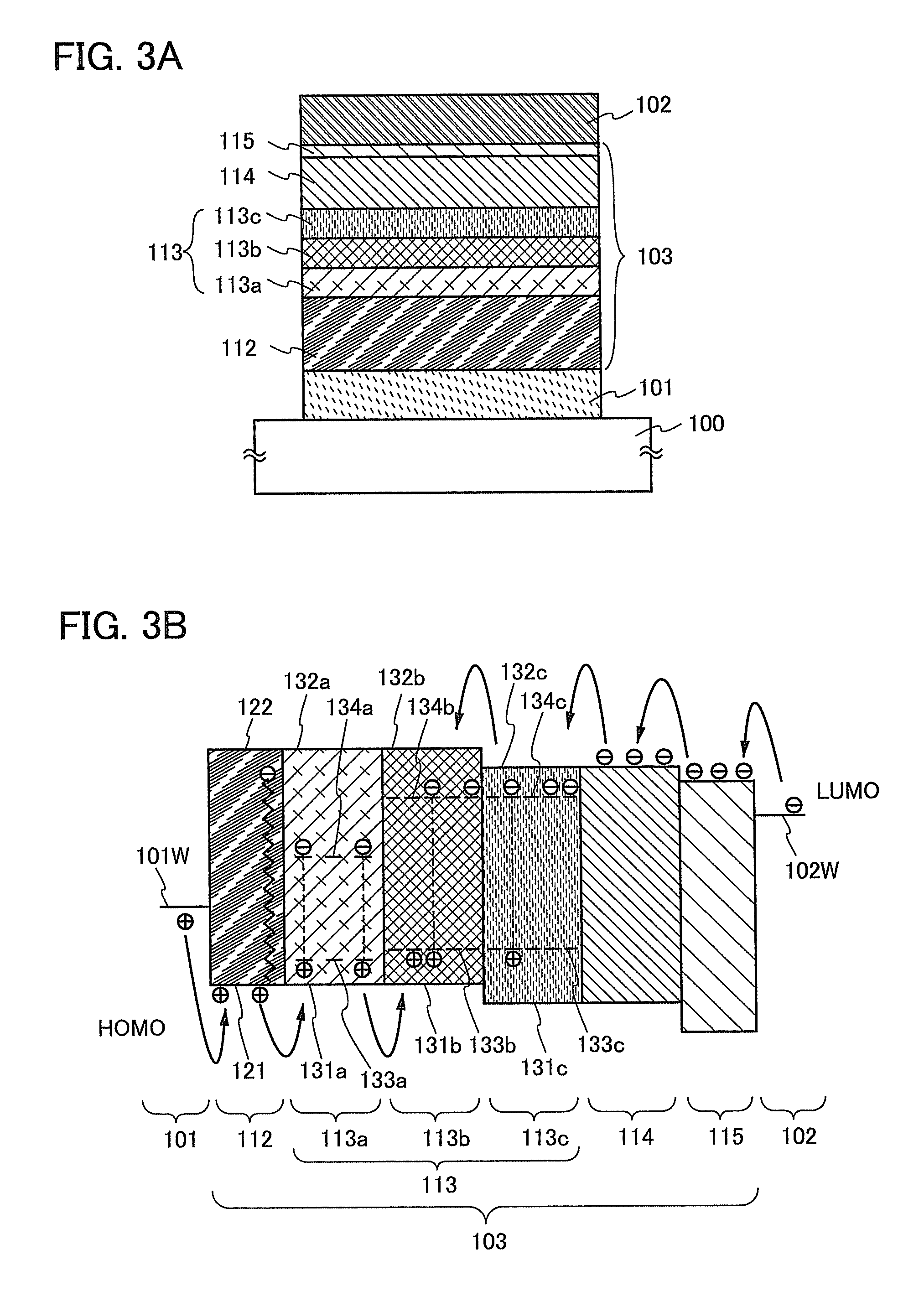
[0182]A light-emitting element which is illustrated in this embodiment includes at least a first light-emitting layer whose one side is in contact with a hole-transport layer, a second light-emitting layer in contact with the other side of the first light-emitting layer, and a third light-emitting layer in contact with a side of the second light-emitting layer on a cathode side. The first light-emitting layer, the second light-emitting layer, and the third light-emitting layer each contain a bipolar host material and a guest material which is a light-emitting material. The guest material contained in the first light-emitting layer has a lower ability for capturing a hole than the guest material contained in the second light-emitting layer, and the guest material contained in the second light-emitting layer has a lower ability for capturing a hole than the guest material contained in the third light-emitting layer. The hole-transport property of the first light-emitting layer is high...
PUM
 Abstract
Description
Claims
Application Information