Method for producing semiconductor device

a semiconductor chip and semiconductor technology, applied in the field of semiconductor chip production, can solve the problems of poor thermal conductivity of materials, heat dissipation, environmental contamination, etc., and achieve the effect of reducing contact thermal resistance, preventing environmental contamination, and efficiently dissipating heat generated in semiconductor chips

Active Publication Date: 2016-02-23
FUJI ELECTRIC CO LTD
View PDF15 Cites 2 Cited by
  • Summary
  • Abstract
  • Description
  • Claims
  • Application Information

AI Technical Summary

Benefits of technology

The present invention aims to provide a low-cost, high-reliability semiconductor device that is designed to be environmentally friendly. The semiconductor device uses lead-free solder for connecting the insulating substrate and the radiating base, as well as the insulating substrate and the semiconductor chip, which prevents the elution of lead from the soldering portions even if the device is placed in an outdoor location. Additionally, the radiating base is solder-connected in a flat state to the insulating substrate, which allows it to be attached to a flat surface of another member without a large gap, while also preventing deterioration of the ceramic board during the attachment step. The lead-free solder also ensures that the semiconductor chip is cooled efficiently, preventing abnormal temperature rise and ensuring stable operation of the semiconductor device. The invention offers a low-cost, high-reliability semiconductor device that works without abnormal temperature rise and can be produced using conventional components, except for the lead-free solder.

Problems solved by technology

However, in production of the above power semiconductor modules, in the case of using a solder for connecting members, particularly members with different heat expansion coefficients, the following problems can result.
When electronic devices and parts using lead-containing solders are discarded, left in an outdoor location, and exposed to acid rain, etc., lead in the solders may be eluted off to cause environment contamination.
However, as compared with copper, these materials are poorer in thermal conductivity and disadvantageous in heat dissipation though they have low heat expansion coefficients.
Further, these materials are more costly than copper.

Method used


Image

  • Method for producing semiconductor device
  • Method for producing semiconductor device
  • Method for producing semiconductor device

Examples


Embodiment Construction

[0042]An embodiment of a power semiconductor module according to the present invention is described in detail below with reference to the drawings.

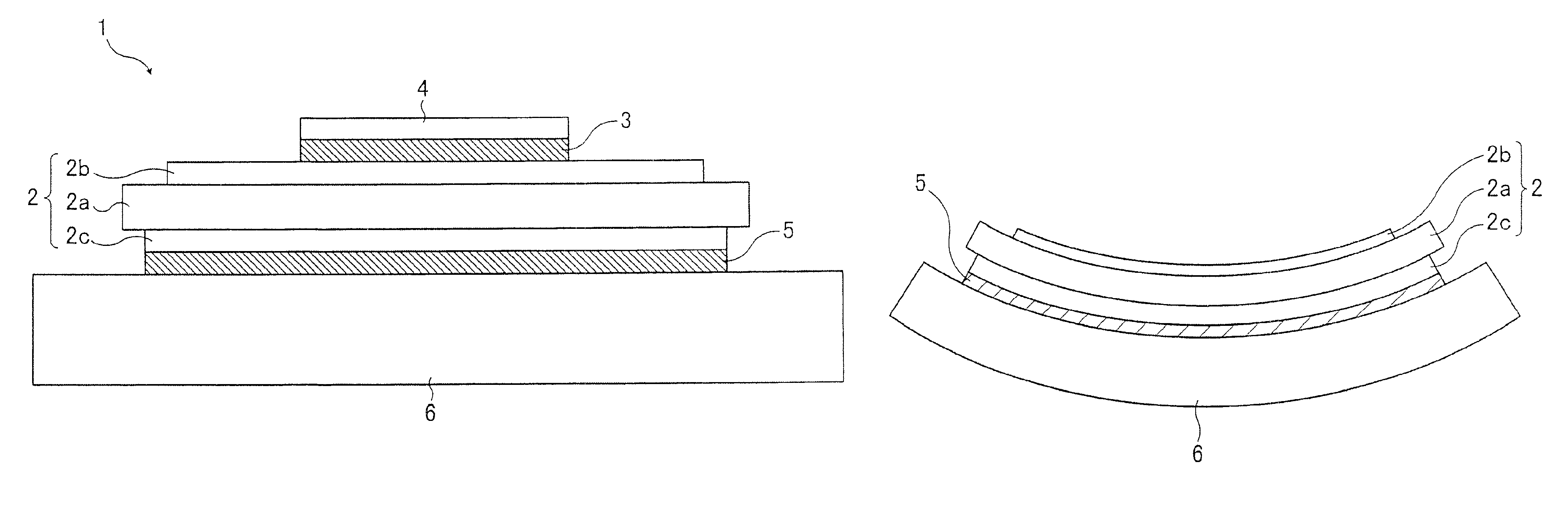
[0043]FIG. 1 is a schematic cross-sectional view showing a principal part of a power semiconductor module.

[0044]In the power semiconductor module 1 shown in FIG. 1, a semiconductor chip 4 is connected by a solder layer 3 onto an insulating substrate 2, which has conductor layers 2b and 2c on the both surfaces of a ceramic board 2a. One surface of the insulating substrate 2 is connected with the semiconductor chip 4 in this manner, and the opposite surface is connected by a solder layer 5 to a radiating base 6.

[0045]For example, the ceramic board 2a for the insulating substrate 2 may be a board mainly composed of alumina (Al2O3) having an appropriate thickness. Further, the conductor layers 2b and 2c may comprise copper foils with appropriate thicknesses.

[0046]For example, the solder layer 3 for connecting the insulating substrate 2 and th...


PUM

PropertyMeasurementUnit
warpageaaaaaaaaaa
warpageaaaaaaaaaa
warpageaaaaaaaaaa

Abstract

A method for producing a semiconductor device includes solder-connecting a semiconductor chip, onto an insulating substrate including a ceramic board and having conductor layers on two surfaces thereof, with a lead-free solder; warping a radiating base such that a surface of the radiating base on a side opposite to the insulating substrate is convex; and solder-connecting the insulating substrate onto the warped radiating base with the lead-free solder so as to provide a substantially flat solder-connected radiating base.

Description

CROSS-REFERENCE TO RELATED APPLICATION[0001]This is a divisional application of Ser. No. 11 / 327,482 filed on Jan. 9, 2006.BACKGROUND OF THE INVENTION AND RELATED ART STATEMENT[0002]The present invention relates to a method of producing a semiconductor device such as a power semiconductor module comprising a power semiconductor.[0003]Power semiconductor modules capable of working even under large current and high voltage have recently been used in various fields. Such power modules comprise a power semiconductor such as an Insulated Gate Bipolar Transistor (IGBT) and a Free Wheeling Diode (FWD) as a main component.[0004]FIG. 11 is a schematic cross-sectional view showing a principal part of a conventional power semiconductor module.[0005]In a power semiconductor module 100 shown in FIG. 11, a semiconductor chip 103 of a power semiconductor, etc. is connected by a solder layer 102 onto an insulating substrate 101, which comprises a ceramic board 101a of aluminum nitride (AlN), etc. an...

Claims


Application Information

Patent Timeline
Patent Type & Authority Patents(United States)
IPC IPC(8): H01L23/00H01L23/373H05K3/00H01L23/34H05K1/03H05K3/34
CPCH01L23/34H01L23/3735H01L24/32H01L24/83H05K3/0061H05K3/3463H01L2224/291H01L2224/29109H01L2224/29111H01L2224/32225H01L2224/83801H01L2924/0103H01L2924/014H01L2924/0105H01L2924/01005H01L2924/01006H01L2924/01013H01L2924/01019H01L2924/01029H01L2924/0132H01L2924/01033H01L2924/0134H01L2924/01042H01L2924/01047H01L2924/01049H01L2924/01051H01L2924/01068H01L2924/01082H01L2924/10253H01L2924/1305H01L2924/13055H01L2924/15787H01L2924/3511H05K1/0306H05K3/341H01L2924/01083H01L2924/00014H01L2924/3512H01L2924/00A41D31/02A41D31/265A41D31/305A41D2400/32A61N2/06
Inventor NISHIMURA, YOSHITAKAMOROZUMI, AKIRAOHNISHI, KAZUNAGAMOCHIZUKI, EIJITAKAHASHI, YOSHIKAZU
Owner FUJI ELECTRIC CO LTD
Why Eureka
Try Eureka