Semiconductor structure and method for manufacturing the same

a technology of semiconductors and semiconductors, applied in the direction of semiconductor devices, basic electric elements, electrical equipment, etc., can solve the problems of reducing the junction depth, and increasing the requirements of device performance for process parameters of source/drain junction extension, etc., to achieve easy control of the junction depth, easy control of the doping concentration, and high doping concentration

Active Publication Date: 2016-03-01
INST OF MICROELECTRONICS CHINESE ACAD OF SCI
View PDF8 Cites 5 Cited by
  • Summary
  • Abstract
  • Description
  • Claims
  • Application Information

AI Technical Summary

Benefits of technology

[0012]The present invention provides a technical solution which has the following advantages: a trench is formed by etching the substrate on both sides of the gate stack, and then a source / drain junction extension is formed in the trench by epitaxial growth and in-situ doping. Compared with the source / drain junction extension formed by the traditional ion implantation, it is easier to control the junction depth of the source / drain junction extension by etching, and it is much easier to control the doping concentration of the source / drain junction extension by in-situ doping during the process of epitaxial growth. Therefore, the present invention can provide a semiconductor structure with a high doping concentration and a low junction depth, thereby effectively improving the performance of the semiconductor structure.

Problems solved by technology

However, decrease in the junction depth of the source / drain junction extension leads to a larger resistance.
However, with the scale-down of IC technology nodes, the requirements of the device performance for process parameters of the source / drain junction extension become increasingly rigorous, especially for the 22 nm or beyond technology.
The difficulties faced by the above technologies are growing.

Method used


Image

  • Semiconductor structure and method for manufacturing the same
  • Semiconductor structure and method for manufacturing the same
  • Semiconductor structure and method for manufacturing the same

Examples


Embodiment Construction

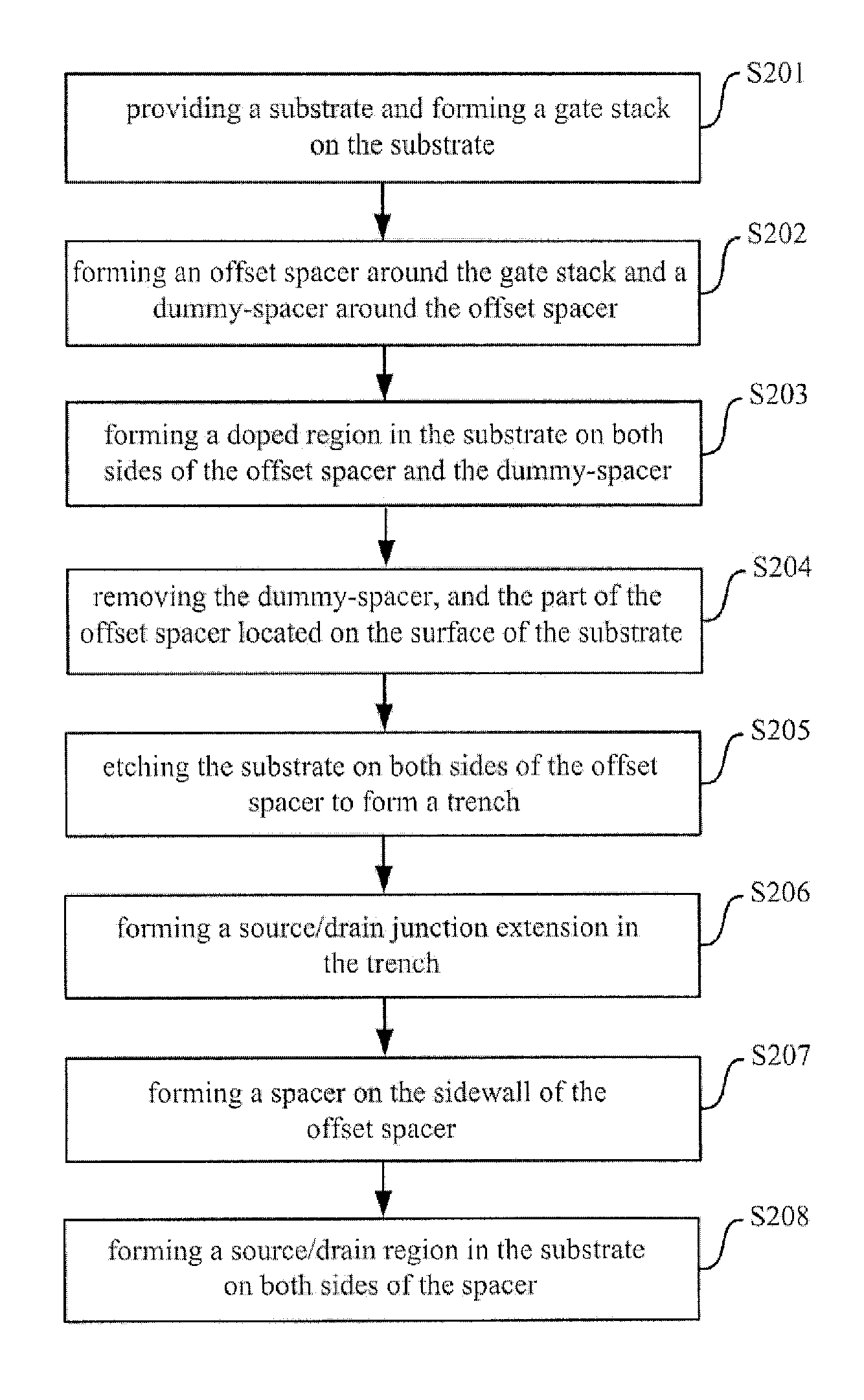
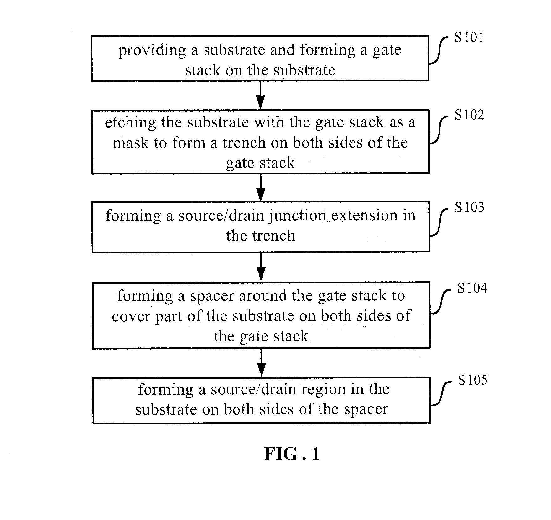
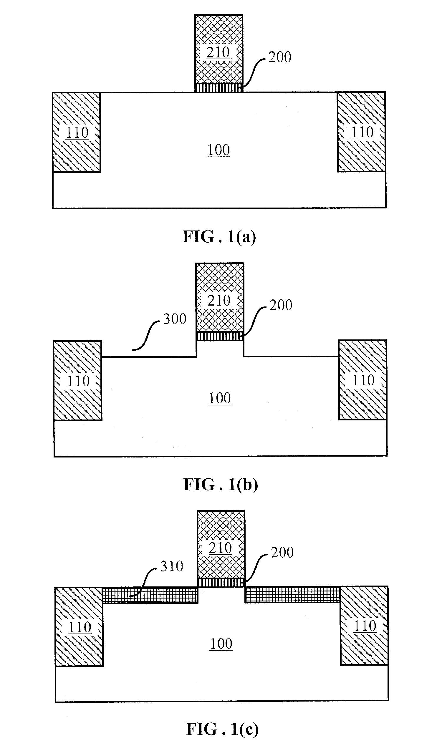
[0020]Exemplary embodiments of the present disclosure will be described in more details.

[0021]Some embodiments are illustrated in the attached drawings, in which the same or similar reference numbers represent the same or similar elements or the components having the same or similar functions. The following embodiments described with reference to the drawings are only exemplary for explaining the present invention, and therefore shall not be construed as limiting the present invention. The disclosure below provides many different embodiments or examples to implement different structures of the present invention. In order to simplify the disclosure of the present invention, components and settings of specific examples are described below. Obviously, they are merely exemplary, and are not intended to limit the present invention. In addition, reference numbers and / or letters can be repeated in different examples of the invention. This repetition is used only for brevity and clarity, an...


PUM


Abstract

The present invention provides a semiconductor structure comprising a substrate; a gate stack on the substrate; a spacer on the sidewalls of the gate stack; a source / drain junction extension formed in the substrate on both sides of the gate stack by epitaxial growth; and a source / drain region in the substrate on both sides of the source / drain junction extension. Accordingly, the present invention also provides methods for manufacturing the semiconductor structure. The present invention can provide a source / drain junction extension with a high doping concentration and a low junction depth, thereby effectively improving the performance of the semiconductor structure.

Description

CROSS REFERENCE TO RELATED APPLICATION[0001]This application is a national stage application, filed under 35 U.S.C. §371, of PCT Application No. PCT / CN2012 / 074776 filed on Apr. 26, 2012, entitled “SEMICONDUCTOR STRUCTURE AND METHOD FOR MANUFACTURING THE SAME”, which claimed priority to Chinese Patent Application Serial No. 201210080996.2 filed on Mar. 23, 2012, all of which are hereby incorporated by reference in their entirety.TECHNICAL FIELD[0002]The present invention relates to the field of semiconductor technology. In particular, the present invention relates to a semiconductor structure and a method for manufacturing the same.BACKGROUND OF THE ART[0003]Source / drain junction extension plays an important role in controlling the short channel effect of MOS devices and improving the device driving capability.[0004]Source / drain junction extension is directly adjacent to the channel conductive region. As the gate length decreases continuously, the junction depth of the source / drain j...

Claims


Application Information

Patent Timeline
Patent Type & Authority Patents(United States)
IPC IPC(8): H01L21/02H01L29/78H01L29/66H01L21/332
CPCH01L29/66575H01L29/6656H01L29/66636H01L29/7833H01L29/6653H01L29/66545
Inventor YIN, HUAXIANGMA, XIAOLONGQI, CHANGLIANGXU, QIUXIACHEN, DAPENG
Owner INST OF MICROELECTRONICS CHINESE ACAD OF SCI
Why Eureka
Try Eureka