Resistive memory and method for fabricating the same

a technology of resistive memory and memory, which is applied in the direction of electrical apparatus, galvano-magnetic device details, etc., can solve the problems of increasing the complexity of peripheral circuits, degrading the stability and reliability and fluctuating key parameters of the resistive material, so as to ensure the stability of various parameters dramatically increase the reliability and stability of the operation of the resistive memory.

Inactive Publication Date: 2016-03-08
PEKING UNIV
View PDF11 Cites 5 Cited by
  • Summary
  • Abstract
  • Description
  • Claims
  • Application Information

AI Technical Summary

Benefits of technology

[0005]Embodiments of the present invention provide a resistive memory and a method for fabricating the same. By means of arranging a conductive protrusion on a bottom electrode of the resistive memory, a “lightning rod” effect is occurred and thus the stability of forming and breaking of a conductive filament are significantly improved.
[0008]It can be seen from the above technical features that, according to the resistive memory provided by the embodiments of the present invention, by means of providing the conductive protrusion on the bottom electrode, a “lightning rod” effect may be occurred so that an electric field in the resistive layer is intensively concentrated near the conductive protrusion. This significantly increases the possibility of generation of the conductive filament at the conductive protrusion, so that the conductive filament is not randomly formed any more. Thus, the stability of various parameters of the resistive memory is ensured, and thus the reliability and stability of the operation of the resistive memory are dramatically increased.

Problems solved by technology

However, numerous key parameters of the resistive material fluctuate greatly due to the randomness of the forming and breaking of the conductive filament.
Such fluctuation significantly degrades the stability and reliability of the operation of the resistive memory and at the same time increases the complexity of peripheral circuits, which becomes a serious obstacle in practical applications.

Method used


Image

  • Resistive memory and method for fabricating the same
  • Resistive memory and method for fabricating the same
  • Resistive memory and method for fabricating the same

Examples


Embodiment Construction

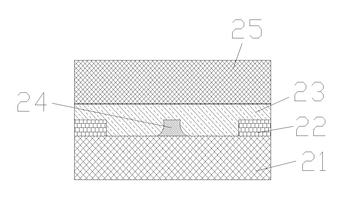
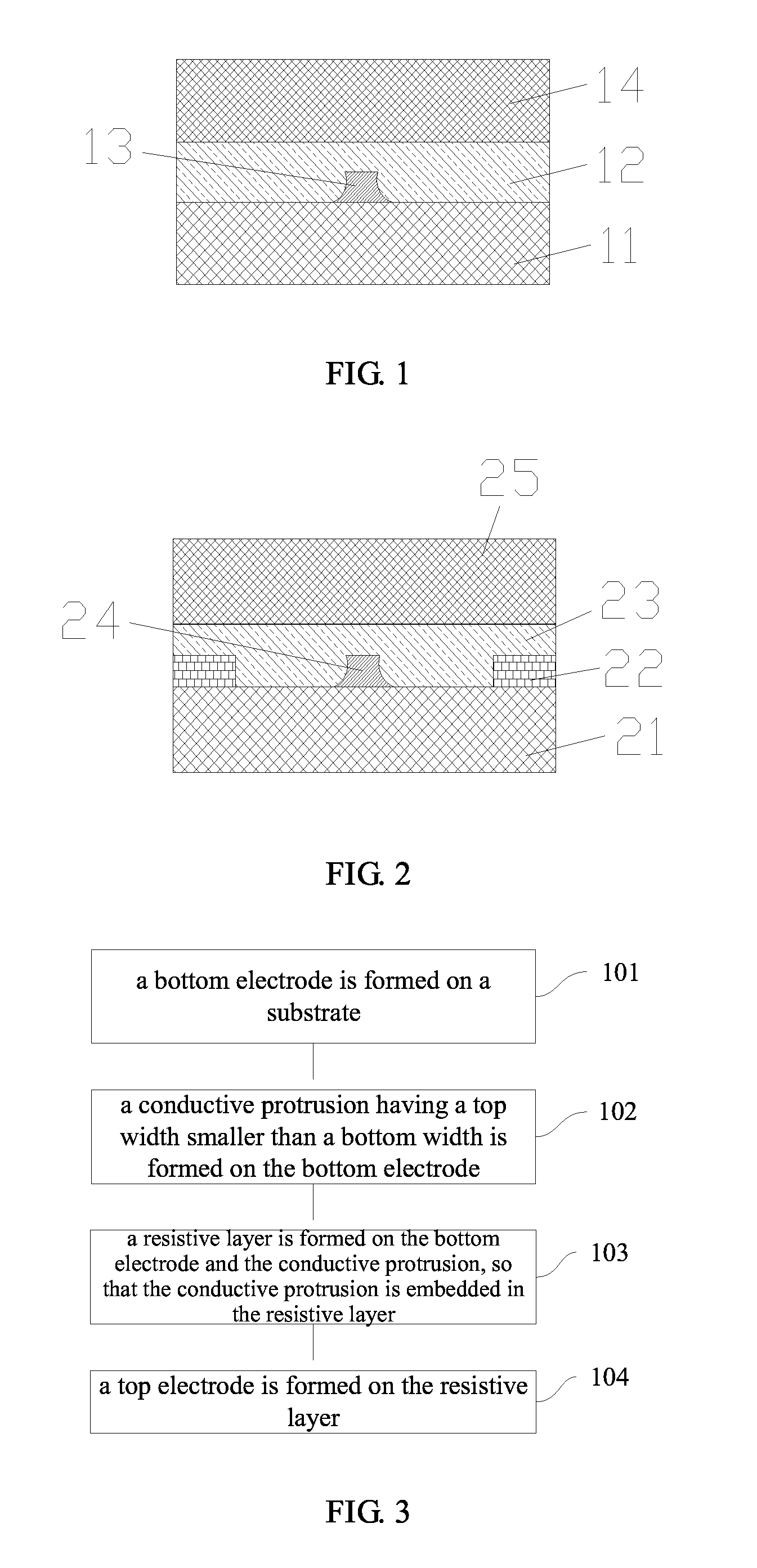
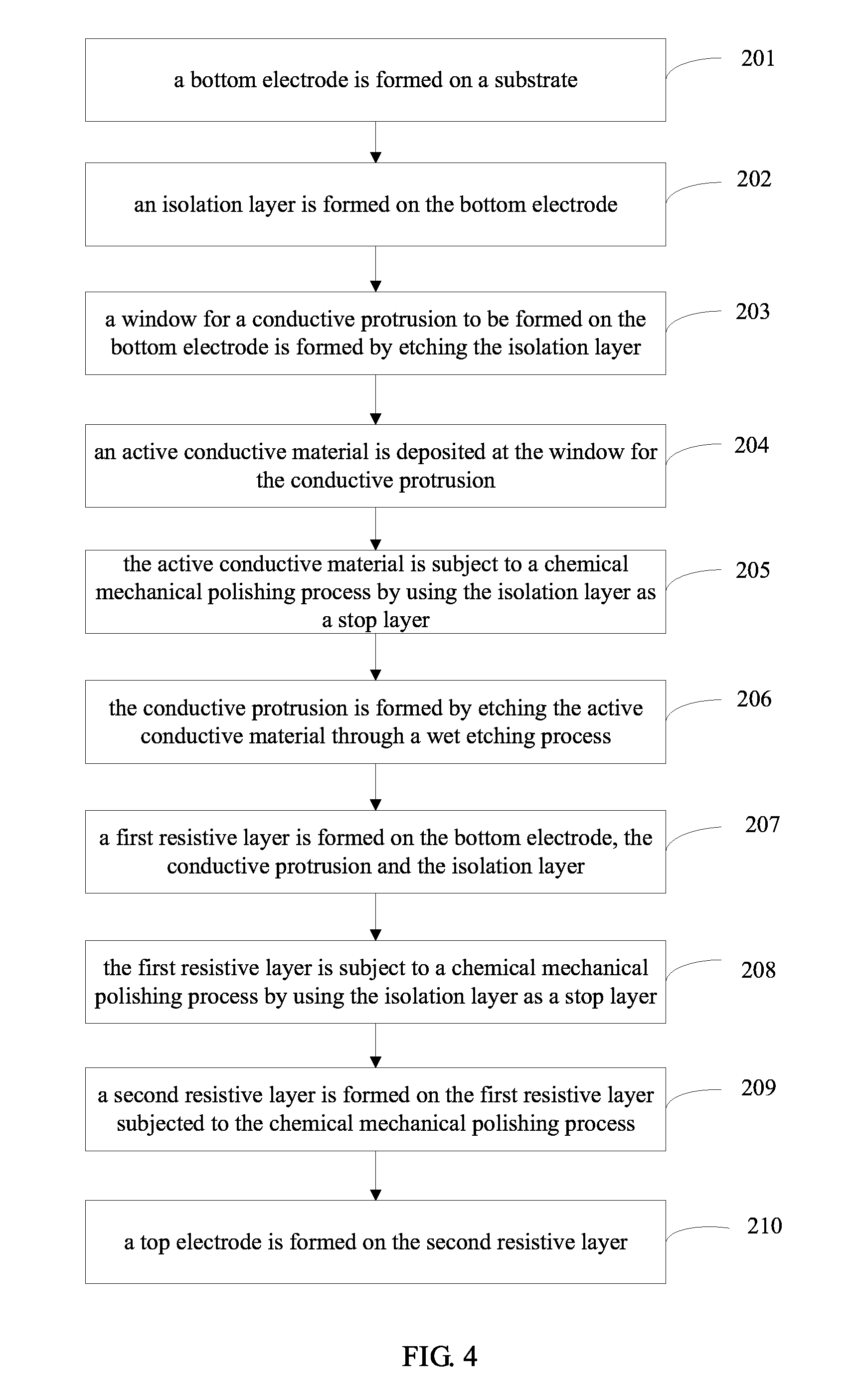
[0016]Hereinafter, the technical solutions in the embodiments of the present invention will be described clearly and thoroughly with reference to the drawings of the embodiments of the present invention. It is apparent that the described embodiments are only part of the implantations of the invention rather than all of them. Based on the embodiments of the present invention, other implantations made by those ordinary persons skilled in the art without any create efforts will fall in the scope of the present invention.

[0017]Moreover, the present invention is described with reference to schematic diagrams. For convenience of descriptions of the embodiments, the cross sectional views illustrating the device structures may not follow the common proportion and may be partially exaggerated. Besides, those schematic diagrams are merely examples, and not intended to limit the scope of the invention. Furthermore, a three-dimensional size including length, width and depth should be considered...


PUM


Abstract

Embodiments of the present invention disclose a resistive memory and a method for fabricating the same. The resistive memory comprises a bottom electrode, a resistive layer and a top electrode. The resistive layer is located over the bottom electrode. The top electrode is located over the resistive layer. A conductive protrusion is provided on the bottom electrode. The conductive protrusion is embedded in the resistive layer, and has a top width smaller than a bottom width. Embodiments of the present invention further disclose a method for fabricating a resistive memory. According to the resistive memory and the method for fabricating the same provided by the embodiments of the present invention, by means of providing the conductive protrusion on the bottom electrode, a “lightning rod” effect may be occurred so that an electric field in the resistive layer is intensively distributed near the conductive protrusion. This significantly increases the possibility of generation of a conductive filament at the conductive protrusion, so that the conductive filament is not randomly formed. Thus, the stability of various parameters of the resistive memory is ensured, and thus the reliability and stability of the operation of the resistive memory are dramatically increased.

Description

CROSS REFERENCE OF RELATED APPLICATIONS[0001]The present application claims priority of Chinese application No. 201210555373.6, filed on Dec. 19, 2012, which is incorporated herein by reference in its entirety.FIELD OF THE INVENTION[0002]The present invention refers to a semiconductor device, and particularly, to a resistive memory and a method for fabricating the same.BACKGROUND OF THE INVENTION[0003]As charge-based non-volatile memories, a flash memory as a representative thereof, is gradually approaching its physical limits, a resistive memory, which is very likely to replace the charge-typed non-volatile memories, has been widely studied during the last decade. Compared to other types of non-volatile memories, the resistive memory has the following advantages: simple structure, fast speed, compatibility with existing fabrication techniques for field effect transistors, potential to be further scaled down and multi-value storage.[0004]A conductive filament theory being as a condu...

Claims


Application Information

Patent Timeline
Patent Type & Authority Patents(United States)
IPC IPC(8): H01L43/02H01L45/00
CPCH01L45/1233H01L45/04H01L45/085H01L45/1253H01L45/1266H01L45/1273H01L45/146H01L45/16H01L45/1608H10N70/245H10N70/20H10N70/8416H10N70/8418H10N70/011H10N70/8833H10N70/826H10N70/021H10N70/841
Inventor CAI, YIMAOYIN, SHIHUIHUANG, RUFANG, YICHEN
Owner PEKING UNIV
Why Eureka
Try Eureka