Film deposition apparatus with low plasma damage and low processing temperature

a film deposition apparatus and plasma damage technology, applied in the field of material deposition technologies, can solve the problems of damage, adversely affecting the electronic performance of the device, damage, etc., and achieve the effects of minimizing or eliminating electronic defects, minimizing or eliminating such damages, and minimizing unwanted effects

Active Publication Date: 2016-04-05
AREESYS TECH
View PDF4 Cites 6 Cited by
  • Summary
  • Abstract
  • Description
  • Claims
  • Application Information

AI Technical Summary

Benefits of technology

[0005]The disclosed deposition apparatus can minimize or eliminate electronic defects produced in or at the interfaces of the devices during thin film deposition. In one example, the disclosed deposition apparatus can minimize or eliminate such damages to OLED during thin film deposition. In another example, the disclosed apparatus can minimize unwanted, uneven bombardment of fast electrons on deposited films which adversely modifies electronic properties of the deposited thin films.
[0006]The disclosed deposition apparatus can provide wider processing windows than conventional deposition systems. For example, the disclosed deposition apparatus can operate under lower processing temperatures and at the same time provide higher plasma density which allows a wider range of desired properties to be achieved in deposited thin films.
[0007]The disclosed deposition apparatus also offers size scalability to process from small to very large substrates.
[0008]Moreover, when configured in a two-sided deposition mode, the disclosed apparatus can double the throughput and materials utilization comparing to a single-sided deposition mode.

Problems solved by technology

However, energetic ions and fast electrons inside the plasma may reach a substrate to cause unwanted damages to thin films already deposited on the substrate, or to electronic devices fabricated in previous process steps.
Such damages may stem from trapped electrical charges inside the deposited films and at their interfaces which can adversely impact the electronic performance of the devices.
The damages may also be caused by other physical degradations or chemical decompositions of delicate materials or sensitive devices due to over-heating by fast electrons and other energetic species, atomic displacement or dislodgment (e.g., milling or sputtering) by energetic ions.
The above described damages can cause OLED device failure when the oxide or nitride thin film is formed by the conventional sputter deposition system 100.

Method used


Image

  • Film deposition apparatus with low plasma damage and low processing temperature
  • Film deposition apparatus with low plasma damage and low processing temperature
  • Film deposition apparatus with low plasma damage and low processing temperature

Examples


Embodiment Construction

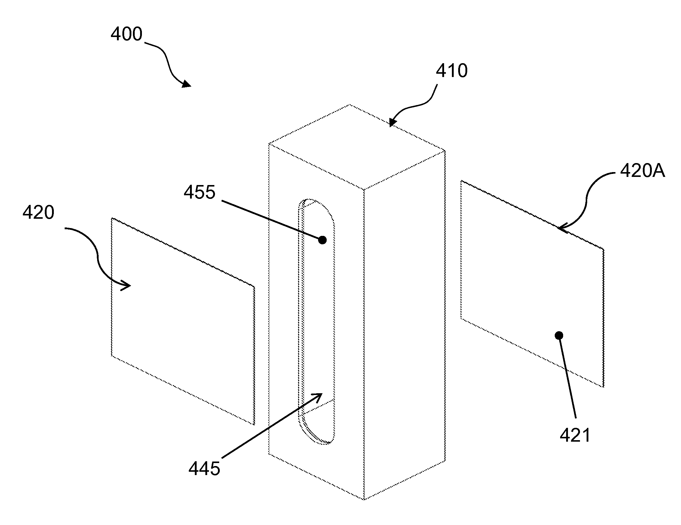
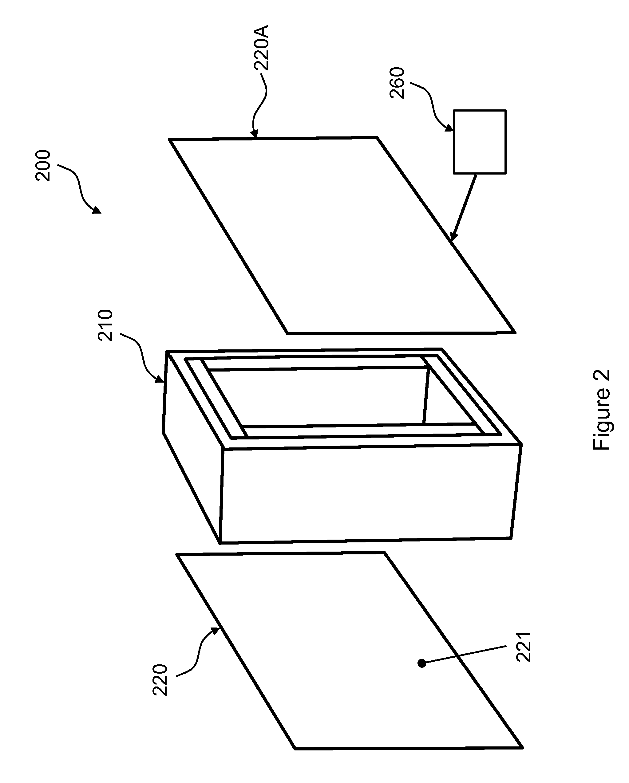
[0022]Referring to FIGS. 2-3, a deposition apparatus 200 includes a magnetron sputter deposition source 210 that is positioned between substrates 220, 220A (i.e. work pieces). The magnetron sputter deposition source 210 is configured to produce vaporized materials that are directed to and deposited onto the substrates 220, 220A. The magnetron sputter deposition source 210 and the substrates 220 are enclosed in a vacuum chamber (not shown for simplicity). The magnetron sputter deposition source 210 is constructed in a backing frame 240 that forms a window 245. Sputtering targets 250 are mounted on the inner surfaces of the backing frame 240, which defines the window 245. In one implementation, the backing frame 240 can be rectangular in shape. The sputtering targets 250 have sputtering surfaces 255 that are aligned substantially perpendicular to the deposition surfaces 221 of the substrates 220, 220A. Thus the window 245 is aligned along an axial direction that is substantially perpe...


PUM

PropertyMeasurementUnit
magnetic fieldaaaaaaaaaa
transparent conductiveaaaaaaaaaa
electronic defectsaaaaaaaaaa

Abstract

A deposition system includes a magnetron sputter deposition source that includes a backing frame that includes a window and a closed loop around the window. The backing frame includes inside surfaces towards the window, one or more sputtering targets mounted on inside surfaces of the backing frame, and one or more magnets mounted on outside surfaces of the backing frame. The one or more sputtering targets include sputtering surfaces that define internal walls of the window. The one or more magnets can produce a magnetic field near the one or more sputtering surfaces. A substrate includes a deposition surface oriented towards the window in the backing frame. The deposition surface receives sputtering material(s) from the one or more sputtering targets.

Description

BACKGROUND OF THE INVENTION[0001]The present application relates to material deposition technologies, and more specifically to sputter deposition systems.[0002]In conventional magnetron sputter deposition systems, a plasma of ions and electrons is created by direct current (DC) or radio frequency (RF) electric excitations. The plasma is confined by a magnetic field to enhance sputtering efficiency. However, energetic ions and fast electrons inside the plasma may reach a substrate to cause unwanted damages to thin films already deposited on the substrate, or to electronic devices fabricated in previous process steps. Such damages may stem from trapped electrical charges inside the deposited films and at their interfaces which can adversely impact the electronic performance of the devices. The damages may also be caused by other physical degradations or chemical decompositions of delicate materials or sensitive devices due to over-heating by fast electrons and other energetic species,...

Claims


Application Information

Patent Timeline
Patent Type & Authority Patents(United States)
IPC IPC(8): H01J37/34C23C14/35
CPCC23C14/35H01J37/3408H01J37/3414H01J37/3417H01J37/3435H01J37/345
Inventor WANG, KAI-ANMARION, CRAIG W.VELAZQUEZ, EFRAIN A.WONG, MICHAEL Z.TING, ALBERTSUN, JINGRU
Owner AREESYS TECH
Why Eureka
Try Eureka