Supercharge Your Innovation With Domain-Expert AI Agents!

Semiconductor device with multiple space-charge control electrodes

a control electrode and space charge technology, applied in the direction of semiconductor devices, basic electric elements, electrical equipment, etc., can solve the problems of limiting the device performance, difficult structure to achieve uniform electric field in the device channel, and difficult efficient control of space charge distribution in the gate-drain spacing

Active Publication Date: 2016-04-12
SENSOR ELECTRONICS TECH
View PDF7 Cites 1 Cited by
  • Summary
  • Abstract
  • Description
  • Claims
  • Application Information

AI Technical Summary

Problems solved by technology

If the space-charge (depletion) region occupies only a portion of the gate-drain spacing, the electric field in that spacing is strongly non-uniform and can result in premature breakdown, which limits the device performance.
Due to a high carrier concentration in the channel and the close vicinity of the channel to the semiconductor surface, efficient control over the space charge distribution in the gate-drain spacing is extremely challenging.
However, even multiple field plate structures cannot achieve a uniform electric field in the device channel.
Additionally, optimal configuration of multiple field plates is difficult to achieve.
In addition, prior art field plates have either source or gate potential applied to them, and therefore significant voltage exists between the field plate and the drain electrode.
As a result, a device including field plate(s) can suffer from premature breakdown between the field plate(s) and the drain electrode.
Furthermore, the field plate(s) increases the inter-electrode and electrode-semiconductor capacitances and therefore decreases the device maximum operating frequency.
As a result of the above limitations, current high-voltage FET switches (i) do not achieve the breakdown voltages predicted by fundamental material properties and (ii) exhibit breakdown voltage-gate-drain spacing dependence saturating at high voltages, typically four hundred volts and above, which imposes serious limitations on device design for kilovolt switching applications.

Method used


Image

  • Semiconductor device with multiple space-charge control electrodes
  • Semiconductor device with multiple space-charge control electrodes
  • Semiconductor device with multiple space-charge control electrodes

Examples


Embodiment Construction

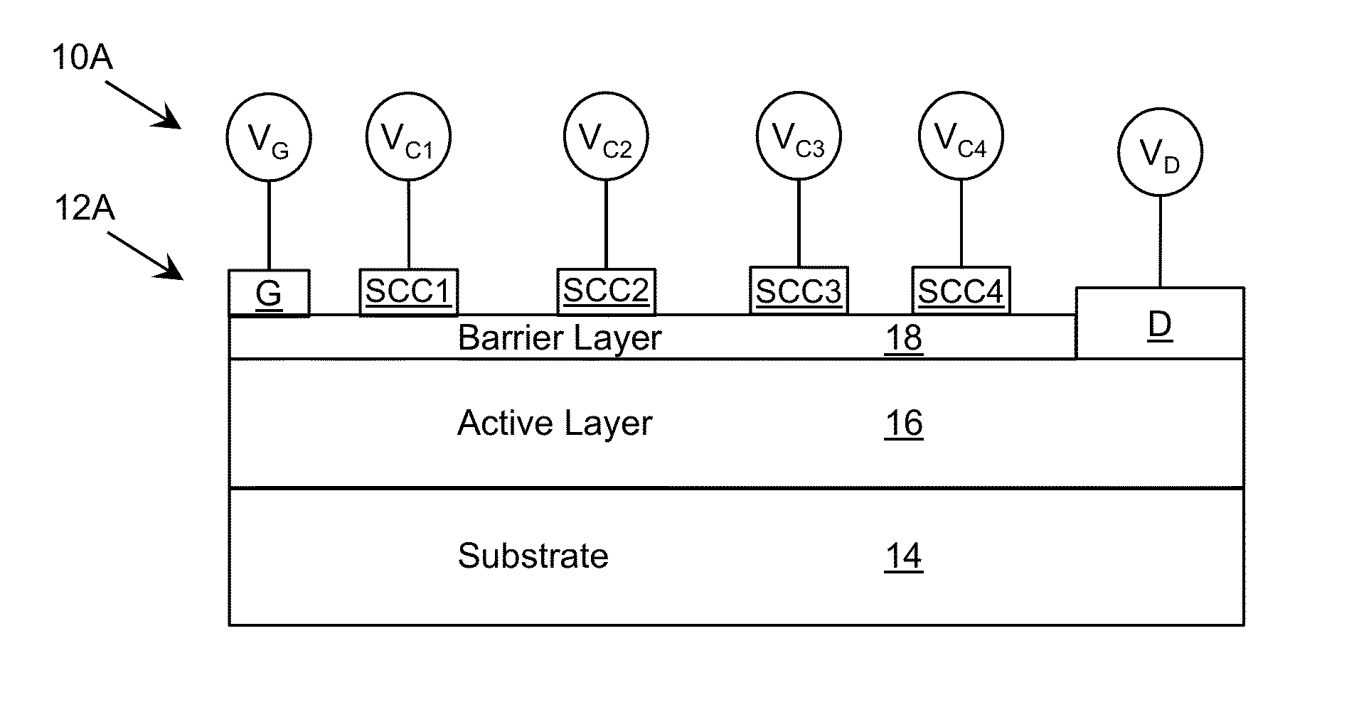
[0026]As indicated above, aspects of the invention provide a circuit including a semiconductor device having a set of space-charge control electrodes. The set of space-charge control electrodes is located between a first terminal, such as a gate or a cathode, and a second terminal, such as a drain or an anode, of the device. The circuit includes a biasing network, which supplies an individual bias voltage to each of the set of space-charge control electrodes. The bias voltage for each space-charge control electrode can be: selected based on the bias voltages of each of the terminals and a location of the space-charge control electrode relative to the terminals and / or configured to deplete a region of the channel under the corresponding space-charge control electrode at an operating voltage applied to the second terminal. Aspects of the invention can provide a solution for increasing an operating voltage and / or a maximum power of the semiconductor device within the circuit. As used h...


PUM


Abstract

A circuit including a semiconductor device having a set of space-charge control electrodes is provided. The set of space-charge control electrodes is located between a first terminal, such as a gate or a cathode, and a second terminal, such as a drain or an anode, of the device. The circuit includes a biasing network, which supplies an individual bias voltage to each of the set of space-charge control electrodes. The bias voltage for each space-charge control electrode can be: selected based on the bias voltages of each of the terminals and a location of the space-charge control electrode relative to the terminals and / or configured to deplete a region of the channel under the corresponding space-charge control electrode at an operating voltage applied to the second terminal.

Description

REFERENCE TO RELATED APPLICATIONS[0001]The current application is a continuation-in-part of U.S. Utility application Ser. No. 14 / 527,203, filed on 29 Oct. 2014, which is a continuation of U.S. Utility application Ser. No. 13 / 682,587 filed on 20 Nov. 2012, now U.S. Pat. No. 8,878,154, which claims the benefit of U.S. Provisional Application No. 61 / 561,980, titled “Semiconductor Device with Multiple Space-Charge Control Electrodes,” which was filed on 21 Nov. 2011, all of which are hereby incorporated by reference. The current application also is a continuation-in-part of U.S. Utility application Ser. No. 13 / 682,139, filed on 20 Nov. 2012, which claims the benefit of U.S. Provisional Application No. 61 / 561,989, filed on 21 Nov. 2011, both of which are hereby incorporated by reference.TECHNICAL FIELD[0002]The disclosure relates generally to semiconductor devices, and more particularly, to a semiconductor device with multiple space-charge control electrodes.BACKGROUND ART[0003]In power ...

Claims


Application Information

Patent Timeline
Patent Type & Authority Patents(United States)
IPC IPC(8): H01L29/02H01L29/40H01L29/423H01L29/417H01L29/778H01L29/872H01L29/06H01L29/20
CPCH01L29/404H01L29/0619H01L29/41725H01L29/42368H01L29/7786H01L29/872H01L29/2003H01L29/405
Inventor SIMIN, GRIGORYSHUR, MICHAELGASKA, REMIGIJUS
Owner SENSOR ELECTRONICS TECH
Features
  • R&D
  • Intellectual Property
  • Life Sciences
  • Materials
  • Tech Scout
  • Unparalleled Data Quality
  • Higher Quality Content
  • 60% Fewer Hallucinations
Learn More