Material for organic electroluminescence device and organic electroluminescence device

a technology of electroluminescence device and material, which is applied in the direction of luminescent compositions, indium organic compounds, organic chemistry, etc., can solve the problems of lowering the probability of short-circuit devices and driving durability, and achieve excellent light-emitting characteristics and reduce the number of short-circuit devices

Active Publication Date: 2016-04-19
UDC IRELAND
View PDF59 Cites 4 Cited by
  • Summary
  • Abstract
  • Description
  • Claims
  • Application Information

AI Technical Summary

Benefits of technology

[0013]An object of the invention is to provide a material for organic electroluminescence device capable of obtaining an organic electroluminescence device with excellent light emitting characteristics and capable of reducing the number of short-circuit devices; and an organic electroluminescence device using the subject material for organic electroluminescence device.
[0016]However, as a result of extensive and intensive investigations made by the present inventor, it has been found that by using, as an organic material to be provided for film formation of any one of layers of at least one organic layer included in an organic electroluminescence device, a material for organic electroluminescence device having a water content before film formation, as measured by the Karl Fischer method, of 100 ppm or more and not more than 1,000 ppm, in an organic electroluminescence device including a layer obtained by film formation of such a material, a probability of occurrence of short-circuit device can be lowered, thereby enhancing the yields without lowering driving durability. The foregoing water content refers to a water content before film formation. Also, at the same time, it has been found that the use of such a material is also effective for suppressing occurrence of cloudiness of the device at the time of device storage. Though mechanisms of these effects have not been elucidated yet, it may be presumed that electrification is suppressed by adsorbed water on the surface of a solid so that attachment of fine dusts to be caused due to the electrification is suppressed. As a result, it may be considered that the inclusion of fine dusts into the device can be suppressed, thereby bringing an effect for reducing an short-circuit device or an enhancement of storage stability.

Problems solved by technology

However, as a result of extensive and intensive investigations made by the present inventor, it has been found that by using, as an organic material to be provided for film formation of any one of layers of at least one organic layer included in an organic electroluminescence device, a material for organic electroluminescence device having a water content before film formation, as measured by the Karl Fischer method, of 100 ppm or more and not more than 1,000 ppm, in an organic electroluminescence device including a layer obtained by film formation of such a material, a probability of occurrence of short-circuit device can be lowered, thereby enhancing the yields without lowering driving durability.

Method used


Image

  • Material for organic electroluminescence device and organic electroluminescence device
  • Material for organic electroluminescence device and organic electroluminescence device
  • Material for organic electroluminescence device and organic electroluminescence device

Examples


examples

[0357]The invention is more specifically described below by reference to the following Examples, but it should not be construed that the scope of the invention is limited to those Examples.

examples 1 to 22

[0358]All of materials used for the preparation of a device were subjected to sublimation purification and confirmed to have a purity (absorption intensity area ratio at 254 nm) of 99.9% or more by means of high-performance liquid chromatography (TSKgel ODS-110Z, manufactured by Tosoh Corporation).

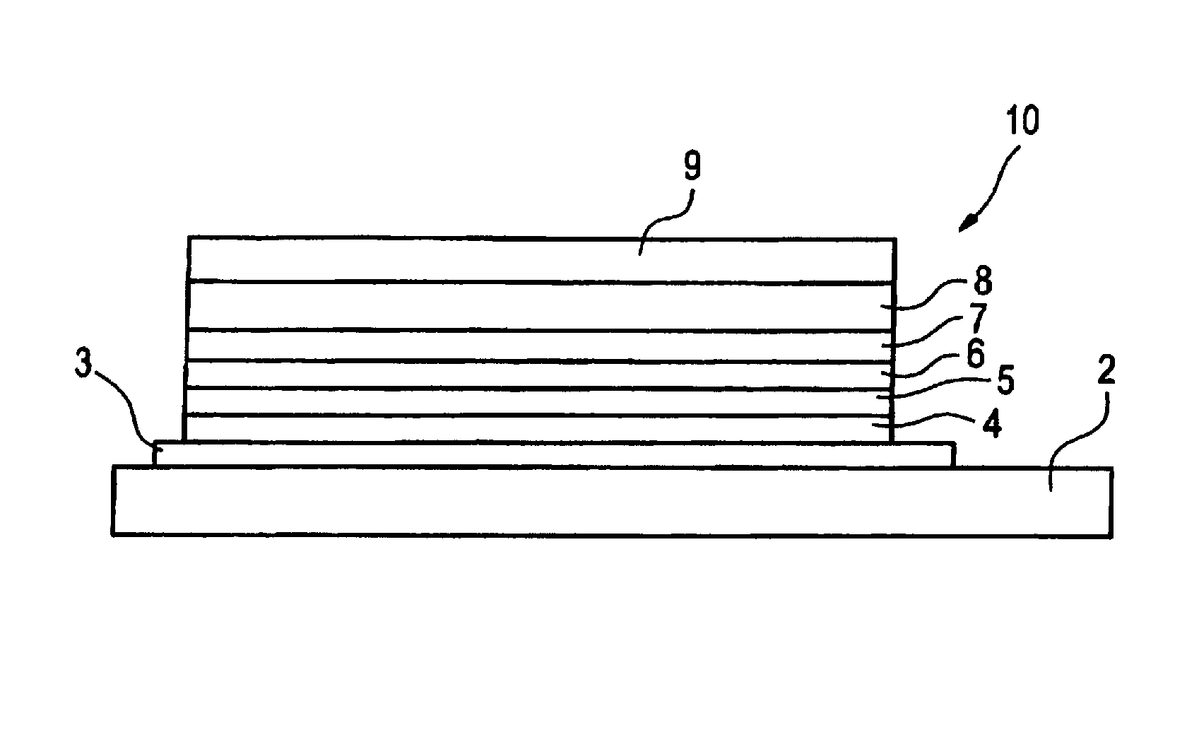
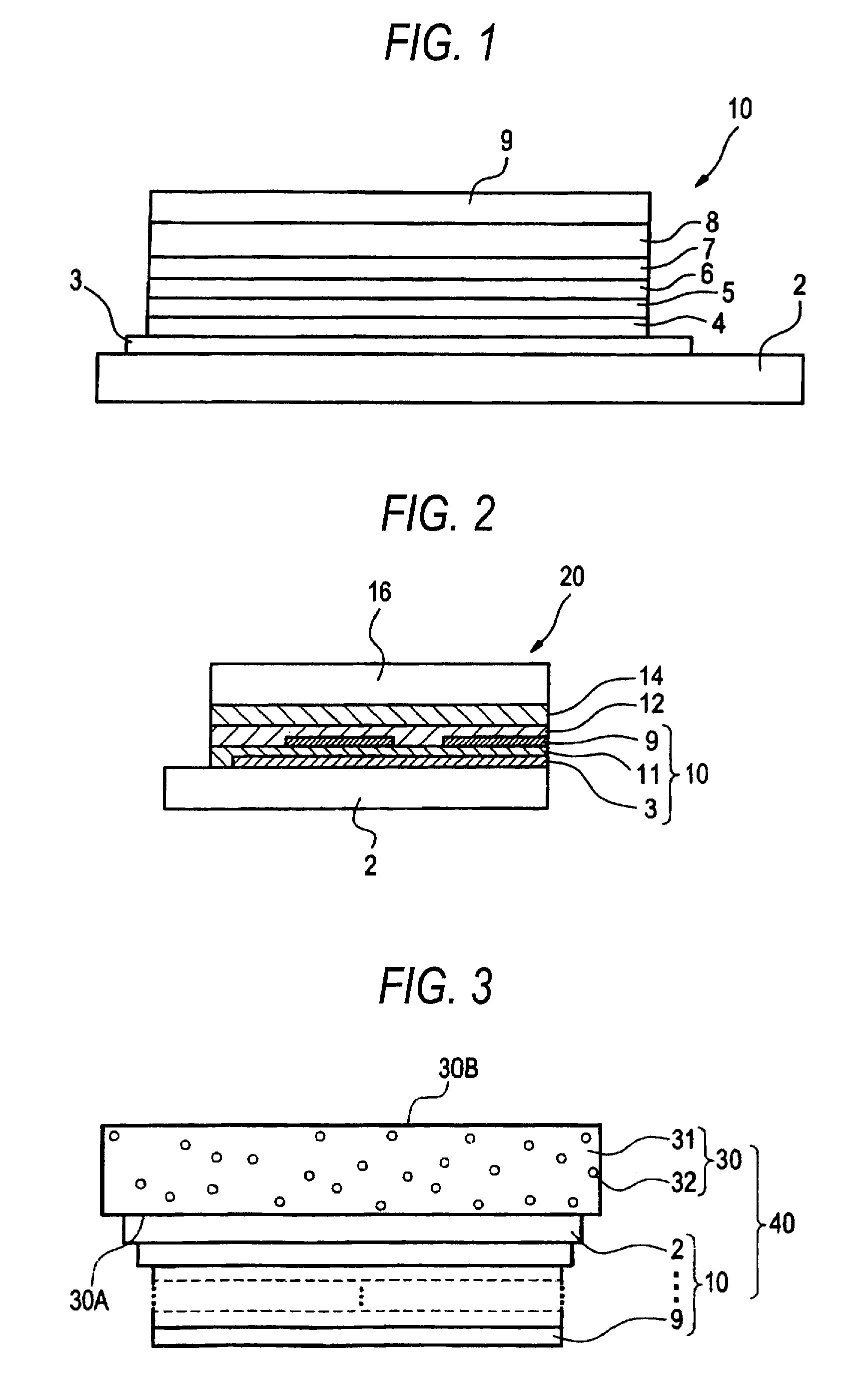
[0359]An indium tin oxide (ITO) film-provided glass substrate having a thickness of 0.5 mm and a size of 2.5 cm in square (manufactured by GEOMATEC Corporation, surface resistance: 10 Ω / □) was put in a washing vessel, ultrasonically washed in 2-propanol and then subjected to a UV-ozone treatment for 30 minutes. The following organic layers were successively vapor deposited on this transparent anode (ITO film) by means of vacuum vapor deposition so as to have each of device configurations shown in Tables 1 to 22.

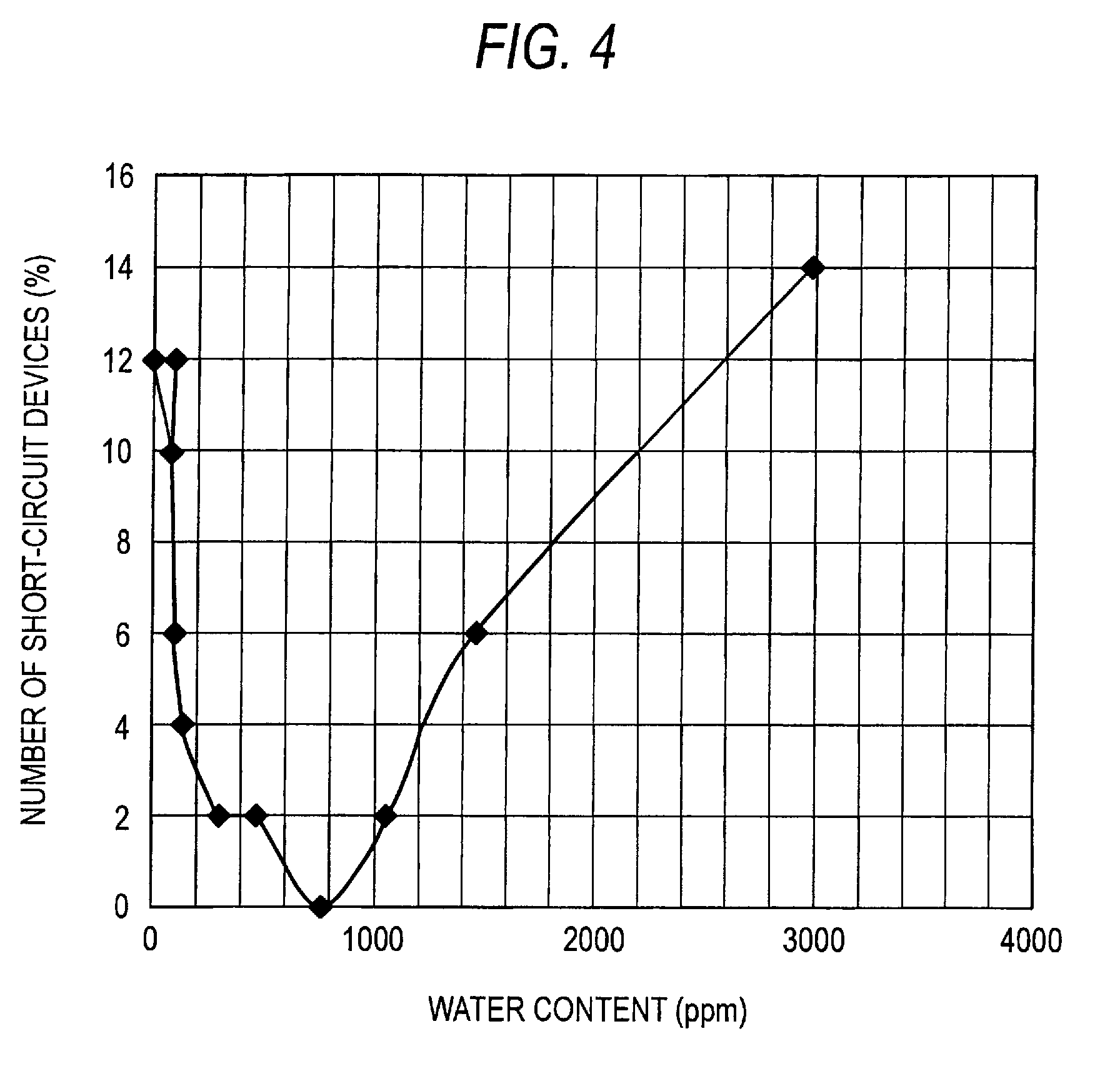
[0360]The devices described in each of Tables 1 to 22 had the same device configuration, except for changing a water content before film formation of a compound as an objective mate...


PUM

PropertyMeasurementUnit
flow rateaaaaaaaaaa
dihedral angleaaaaaaaaaa
thicknessaaaaaaaaaa

Abstract

A material for an organic electroluminescence device, includes: an organic material that is to be provided for a film formation of any of at least one organic layer included in the organic electroluminescence device, the organic material having a water content before the film formation, as measured by the Karl Fischer method, of 100 ppm or more and not more than 1,000 ppm.

Description

BACKGROUND OF THE INVENTION[0001]1. Field of the Invention[0002]The present invention relates to a material for organic electroluminescence device and an organic electroluminescence device (hereinafter also referred to as “device” or “organic EL device”). The invention relates to a technology capable of reducing a rate of occurrence of short-circuit device in the manufacture and enhancing manufacturing yields and a technology capable of enhancing storage stability of the device.[0003]2. Description of the Related Art[0004]In recent years, in view of the fact that light emission with a high brightness is obtainable through low-voltage driving, an organic electroluminescence device has been actively researched and developed. In general, the organic electroluminescence device is constituted of an organic layer including a light emitting layer and a pair of electrodes interposing this light emitting layer therebetween, and energy of an exciton generated through recombination of an elect...

Claims


Application Information

Patent Timeline
Patent Type & Authority Patents(United States)
IPC IPC(8): C09K11/06C07D209/86H01L51/00H01L51/50H01L51/52C07F15/00
CPCH01L51/0085C07D209/86C09K11/06C07F15/0033C09K2211/1007C09K2211/1011C09K2211/1029C09K2211/1044C09K2211/185H01L51/0072H01L51/5016H01L51/5268H10K85/342H10K50/11H10K2101/10H10K50/854H10K50/12H10K50/15H10K50/16H10K50/17H10K50/18H10K50/171H10K71/00H10K85/6572
Inventor ISE, TOSHIHIRO
Owner UDC IRELAND
Why Eureka
Try Eureka