Semiconductor device and method for manufacturing the same

a technology of semiconductors and semiconductors, applied in the direction of optical waveguide light guides, instruments, optics, etc., can solve the problems of difficult to obtain a good quality crystalline film, difficult to obtain the large amount of thickness variation with high accuracy, etc., and achieve the effect of large thickness variation and high accuracy

Active Publication Date: 2016-05-31
SUMITOMO ELECTRIC IND LTD
View PDF1 Cites 0 Cited by
  • Summary
  • Abstract
  • Description
  • Claims
  • Application Information

AI Technical Summary

Benefits of technology

[0006]The present invention provides a method for manufacturing a semiconductor device including the steps of preparing a substrate having a first region, a second region, a third region, and a fourth region; forming a first layer on the substrate and a second layer on the first layer; forming a suspended mask on the substrate by etching the first layer and the second layer, the suspended mask including a shield portion having a space between the second layer and the substrate at the first region, a terrace portion being disposed apart from the shield portion at the second region, a supporting portion connecting the shield portion and the terrace portion at the third region, and an opening between the shield portion and the terrace portion at the fourth region, the shield portion extending in a first direction; and growing a semiconductor layer on a surface of the substrate in the first region and the fourth region using the suspended mask. The shield portion of the suspended mask has a width varying in the first direction, and the semiconductor layer has a thickness varying in the first direction. In accordance with the present invention, a semiconductor layer whose thickness is varied in the first direction is obtained without defects such as cross-hatch. The shield portion extending along the first direction has enough length for a spot-size converter, The first direction is used as the longer direction of a waveguide for the spat-size converter. Furthermore, the amount of variation in the thickness can be large with high accuracy.

Problems solved by technology

However, in crystal growth using along shadow mask, it is difficult to obtain a good quality crystalline film.
Furthermore, it is difficult to obtain the large amount of variation in the thickness with high accuracy.

Method used


Image

  • Semiconductor device and method for manufacturing the same
  • Semiconductor device and method for manufacturing the same
  • Semiconductor device and method for manufacturing the same

Examples


first embodiment

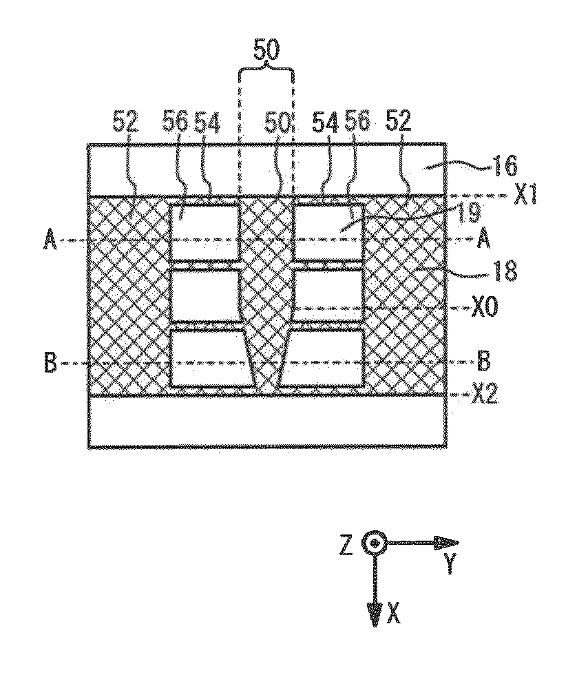
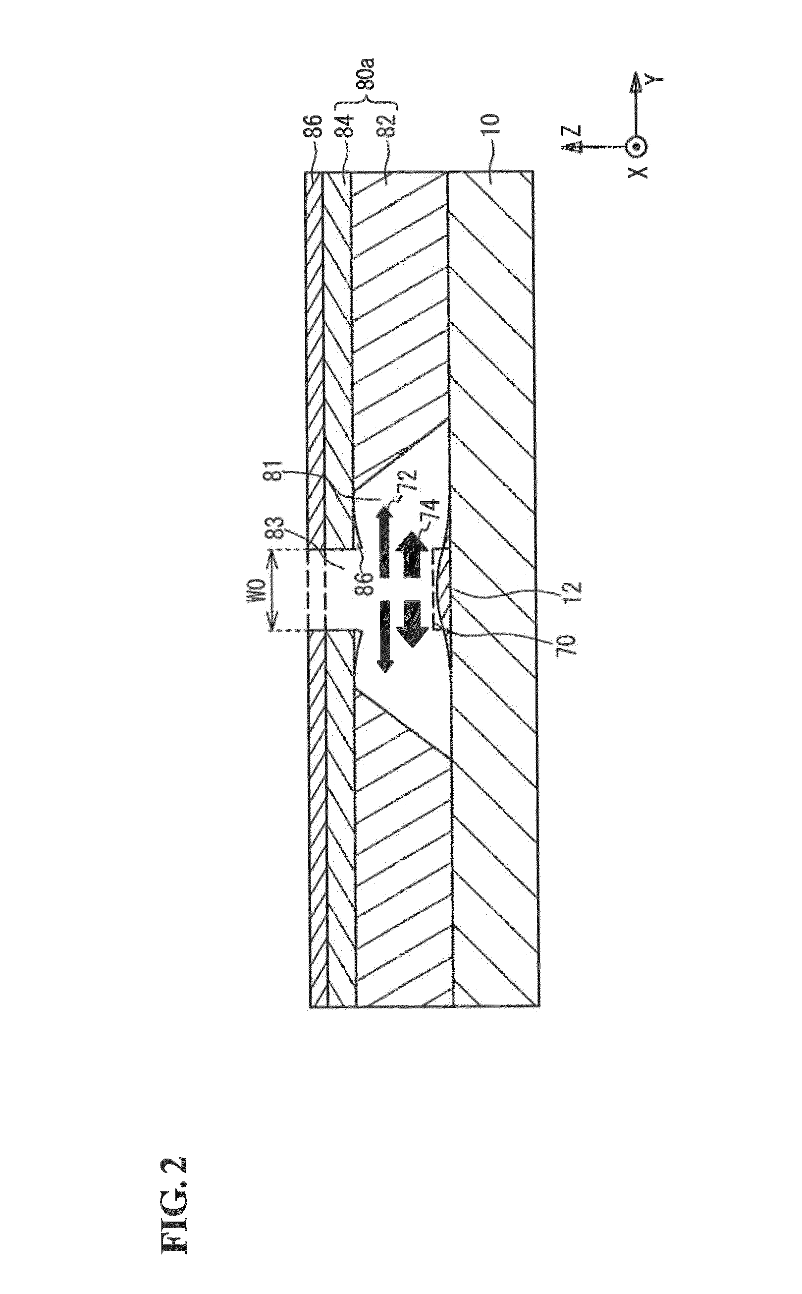
[0072]FIG. 5A is a plan view of a suspended mask 80 of the first embodiment in the present invention. FIG. 5B is a graph showing the relationship between the thickness T1 of the semiconductor layer formed using the suspended mask 80 and the position X. The thickness is taken along the line D-D of FIG. 5A. FIGS. 6A to 6C are a cross-sectional view taken along the line A-A of FIG. 5A, a cross-sectional view taken along the line BB of FIG. 5A, and a cross-sectional view taken along the line C-C of FIG. 5A, respectively, Referring to FIG. 5A, the suspended mask 80 is formed in a first region 50, a second region 52, a third region 54 and a fourth region 56. Referring to FIGS. 6A to 6C, the suspended mask 80 includes a first layer 14 and a second layer 16.

[0073]As shown in FIG. 5A, the first region 50 extends in the X direction, and the width W1 in the Y direction is changed along the X direction. The X direction corresponds to the first direction, and the Y direction corresponds to the s...

second embodiment

[0143]A semiconductor layer formed in the first embodiment is used in a waveguide for a spot-size converter. FIG. 16 is a block diagram of a system in which a semiconductor device 100 according to a second embodiment is used. As shown in FIG. 16, spot-size converters 91 and 92, a Mach-Zehnder modulator 93, waveguides 94 and 95, and an interconnection 102 are disposed on a substrate 90. The spot-size converters 91 and 92, the Mach-Zehnder modulator 93, the waveguides 94 and 95 and the substrate 10 are composed of semiconductors. The interconnection 102 is composed of a metal. A laser light 98 is radiated from a lensed fiber 96 onto the spot-size converter 91. The spot-size converter 91 converts the spot site of the laser light 98 into the size of the waveguide 95. The Mach-Zehnder modulator 93 modulates an optical signal propagated through the waveguide 94 using an electrical signal 103 propagated through the interconnection 102. The Mach-Zehnder 93 outputs a modulated light to the w...

third embodiment

[0165]FIGS. 33A to 33C shows the shape of a suspended mask 80g of the third embodiment. FIGS. 33A to 33C are cross-sectional views showing the process of forming a semiconductor layer in accordance with a third embodiment. FIGS. 33A to 33C show a first region 50 and fourth regions 56. In the third embodiment, a second layer 16a is made of an insulating layer. As the second layer 16a, for example, a silicon dioxide film or a silicon nitride film is used. In FIGS. 33A to 33C, the solid line in the semiconductor layer 12 indicates the surface of the semiconductor layer 12 formed using the suspended mask 80g. The broken line indicate the semiconductor layer 12 of the first embodiment in which the second layer 16 is composed of a semiconductor.

[0166]When the second layer 16a is formed of an insulating layer, no semiconductor layer is formed around the second layer 16a. On the other hand, as shown in FIGS. 6A to 6C in the first embodiment, the semiconductor layer 86 is formed on and under...


PUM


Abstract

A method for manufacturing a semiconductor device includes the steps of preparing a substrate; forming first and second layers on the substrate; forming a suspended mask on the substrate by etching the first and second layers, the suspended mask including a shield portion having a space between the second layer and the substrate, a terrace portion being disposed apart from the shield portion, a supporting portion connecting the shield portion and the terrace portion, and an opening between the shield portion and the terrace portion, the shield portion extending in a first direction; and growing a semiconductor layer on a surface of the substrate in the first region and the fourth region using the suspended mask. The shield portion has a width varying in the first direction, and the semiconductor layer has a thickness varying in the first direction.

Description

BACKGROUND OF THE INVENTION[0001]1. Field of the Invention[0002]The present invention relates to a semiconductor device and a method for manufacturing the same, and relates to a semiconductor device in which a semiconductor layer is deposited on a substrate, and a method for manufacturing the same.[0003]2. Description of the Related Art[0004]A semiconductor layer deposited on a substrate is used as an optical waveguide, Patent Document 1 (Japanese Unexamined Patent Application Publication No. 10-135563) describes a semiconductor layer whose thickness is varied, The variation of the thickness is formed by crystal growth using a shadow mask. The semiconductor layer whose thickness is varied is used as a waveguide, In the method of Patent Document 1, the thickness of the semiconductor layer is varied in the width direction of the waveguide,SUMMARY OF THE INVENTION[0005]In order to apply the waveguide to a spot-size convert, it is necessary to vary the thickness in the longer direction ...

Claims


Application Information

Patent Timeline
Patent Type & Authority Patents(United States)
IPC IPC(8): G02B6/12G02B6/136G02B6/122H01L21/02G02B6/13
CPCG02B6/1228G02B6/131G02B6/136H01L21/02546H01L21/02639H01L21/02664G02B2006/12097H01L21/02543H01L21/0262
Inventor HORINO, KAZUHIKO
Owner SUMITOMO ELECTRIC IND LTD
Why Eureka
Try Eureka