Dye-sensitized photoelectric conversion device and method of manufacturing the same

a technology of photoelectric conversion device and dye sensitization, which is applied in the manufacture of final products, basic electric elements, electrolytic capacitors, etc., can solve the problems of increasing dependence on these kinds of energy, increasing the risk of radioactive contamination of atomic energy, and increasing the risk of atomic energy use, so as to reduce the strength and durability. , the effect of preventing the provision of such a feed por

Inactive Publication Date: 2010-04-29
SONY CORP
View PDF28 Cites 106 Cited by
  • Summary
  • Abstract
  • Description
  • Claims
  • Application Information

AI Technical Summary

Benefits of technology

[0039]According to the present invention constituted as above-mentioned, the end sealing step required for filling with an electrolyte in the case of a dye-sensitized photoelectric conversion device according to the related art is unnecessitated, and the need to provide a substrate with a feed port for injecting the electrolyte is eliminated. Therefore, lowering in strength and durability due to the provision of such a feed port can be prevented. Further, the problem of generation of a projection is also obviated, owing to the absence of an end-sealed portion.
[0040]According to the present invention, a dye-sensitized photoelectric conversion device being excellent in strength and durability and free of any projection can be manufactured through simple manufacturing steps.

Problems solved by technology

It is said that when a fossil fuel such as coal and petroleum is used as an energy source, the resulting carbon dioxide leads to global warming.
Besides, the use of atomic energy is attended by the risk of radioactive contamination.
As the environmental issues are much talked about at present, dependence on these kinds of energy involves many problems.
However, although the crystalline silicon solar cells are superior to the amorphous silicon solar cells in photoelectric conversion efficiency, which represents the performance of converting the light (solar) energy into electrical energy, the crystalline silicon solar cells are low in productivity and disadvantageous on a cost basis because much energy and time are needed for crystal growth.
In addition, although the amorphous silicon solar cells are characterized by higher light absorption properties, a wider range of substrate choice and an easier increase in area as compared with the crystalline silicon solar cells, the amorphous silicon solar cells are inferior to the crystalline silicon solar cells in photoelectric conversion efficiency.
Further, though the amorphous silicon solar cells are higher in productivity than the crystalline silicon solar cells, the production of the amorphous silicon solar cells needs a vacuum process, like in manufacturing the crystalline silicon solar cells, so that the cost of equipment is still high.
Such solar cells, however, have very low photoelectric conversion efficiencies of 1% or below and are unsatisfactory in durability.
However, the above-mentioned dye-sensitized solar cells in the past have problems as to the end-sealed portion strength and durability, and, in addition, have a shape-basis demerit in that a projection is generated due to the end-sealed portion.

Method used


Image

  • Dye-sensitized photoelectric conversion device and method of manufacturing the same
  • Dye-sensitized photoelectric conversion device and method of manufacturing the same
  • Dye-sensitized photoelectric conversion device and method of manufacturing the same

Examples


example 1

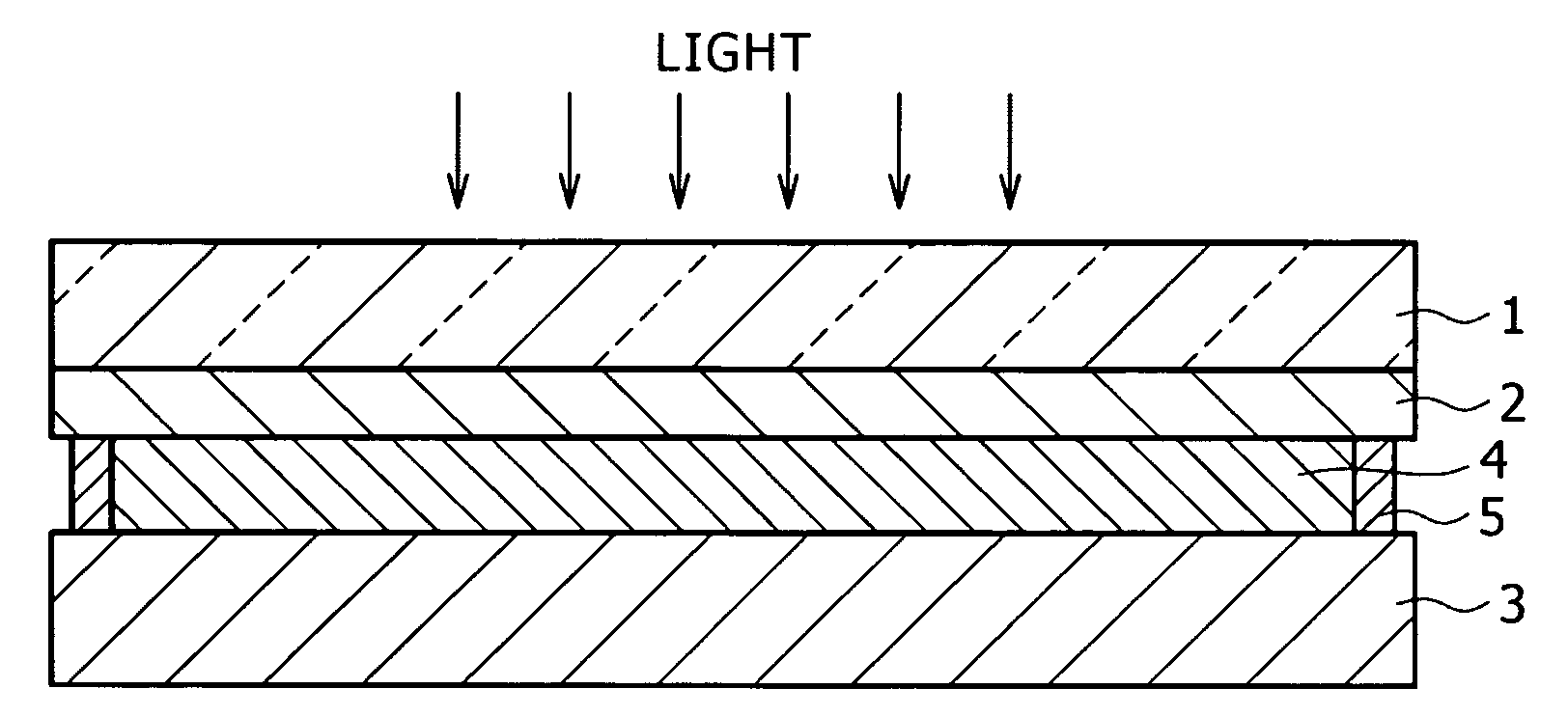
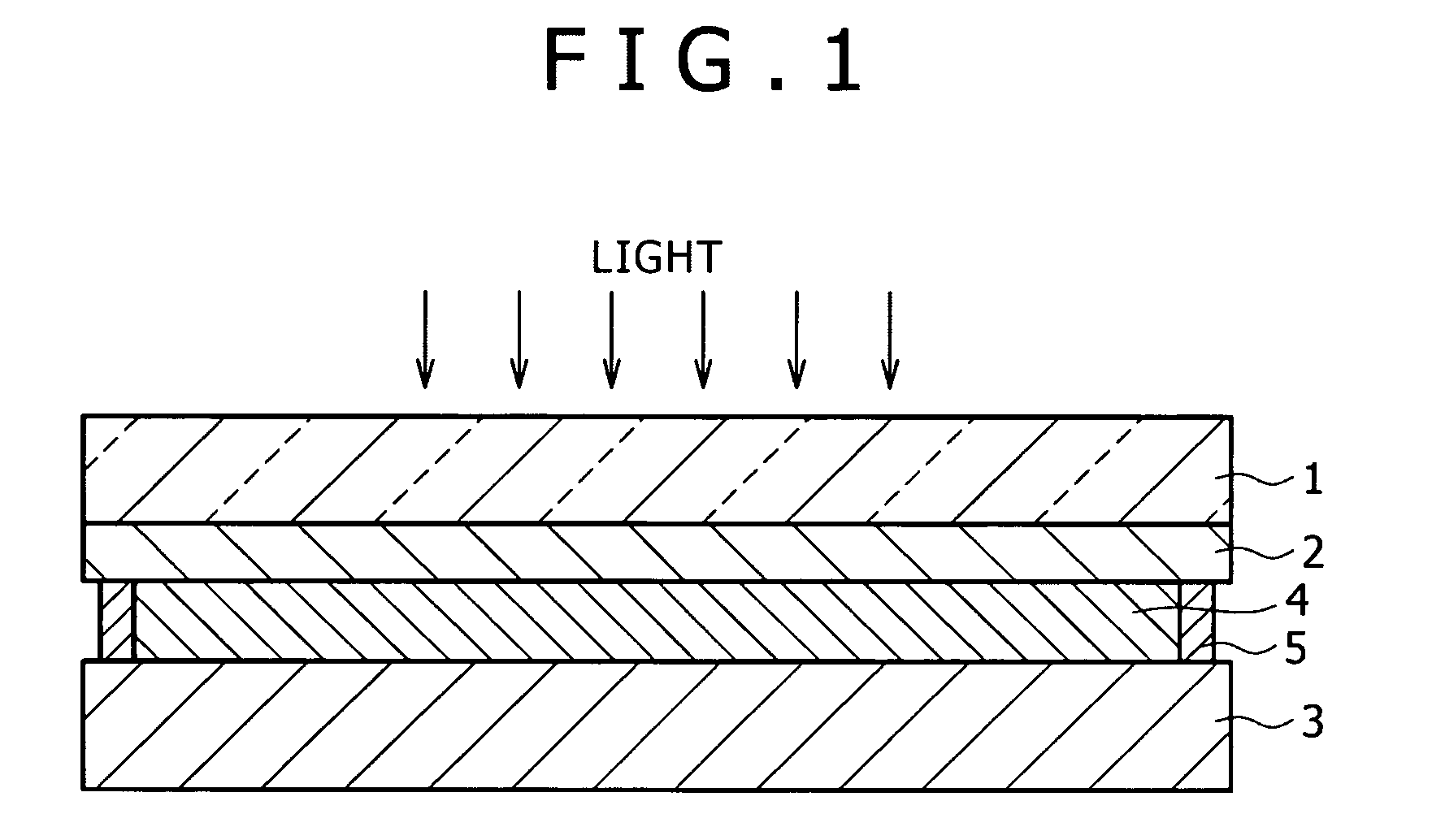
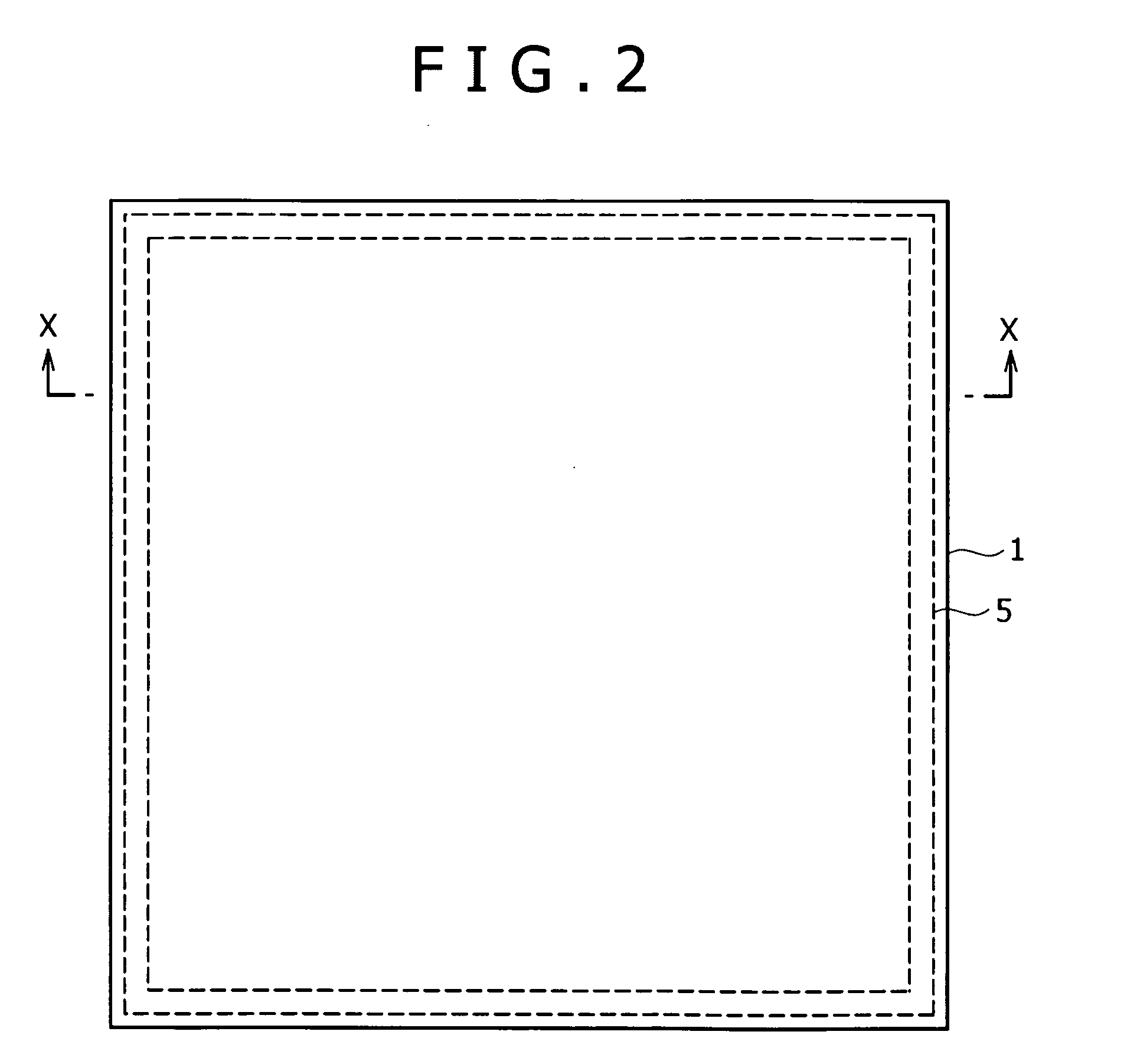
[0067]A transparent conductive substrate was prepared as follows. An FTO substrate (sheet resistance: 10Ω / □) for use in amorphous solar cell, produced by Nippon Sheet Glass Co., Ltd., was processed into the size of 25 mm×25 mm×(t) (thickness 1.1 mm), and the processed FTO substrate was then subjected to ultrasonic cleaning by sequentially using acetone, an alcohol, an alkali cleaning liquid, and ultrapure water, followed by drying.

[0068]The FTO substrate was coated with a titanium oxide paste, produced by Solaronix, by use of a screen printing machine with a screen mask shaped to have a diameter of 5 mm. In coating with the paste, a 7 μm-thick layer of a transparent Ti-Nanoxide TSP paste and a 13 μm-thick layer of Ti-Nanoxide DSP containing scattering particles were sequentially formed in this order from the FTO substrate side, to obtain a porous titanium oxide film in a total thickness of 20 μm. The porous titanium oxide film was baked in an electric furnace at 500° C. for 30 min, ...

example 2

[0089]After forming an FTO film on a glass substrate, the FTO film was patterned by etching to form an eight-stripe pattern with 0.5 mm-wide gaps between the stripes. Thereafter, the resulting assembly was subjected to ultrasonic cleaning by sequentially using acetone, an alcohol, an alkali cleaning liquid, and ultrapure water, followed by sufficient drying.

[0090]A titanium oxide paste produced by Solaronix was applied onto the glass substrate in an eight-stripe pattern, each stripe measuring 5 mm in width and 40 mm in length (total area: 16 cm2) by use of a screen printing machine. In applying the paste, a 7 μm-thick layer of a transparent Ti-Nanoxide TSP paste and a 13 μm-thick layer of Ti-Nanoxide DSP containing scattering particles were sequentially formed in this order from the glass substrate side, to obtain a porous TiO2 film in a total thickness of 20 μm. The porous TiO2 film was baked in an electric furnace at 500° C. for 30 min, and allowed to cool. Thereafter, the porous ...

example 3

[0114]After forming an FTO film on a glass substrate, the FTO film was patterned by etching to form an eight-stripe pattern. Thereafter, the resulting assembly was subjected to ultrasonic cleaning by sequentially using acetone, an alcohol, an alkali cleaning liquid, and ultrapure water, followed by sufficient drying.

[0115]A titanium oxide paste produced by Solaronix was applied onto the glass substrate in a pattern of eight stripes, each measuring 5 mm in width and 40 mm in length (total area: 16 cm2), by use of a screen printing machine. In applying the paste, a 7 μm-thick layer of a transparent Ti-Nanoxide TSP paste and a 13 μm-thick layer of Ti-Nanoxide DSP containing scattering particles were sequentially formed in this order from the glass substrate side, to obtain porous titanium oxide films in a total thickness of 20 μm. The porous titanium oxide films were baked in an electric furnace at 500° C. for 30 min, and allowed to cool. Thereafter, the porous titanium oxide films wer...


PUM


Abstract

A method of manufacturing a dye-sensitized photoelectric conversion device is provided by which a dye-sensitized photoelectric conversion device being excellent in strength and durability and free of any projection, as a result of the absence of need for an end seal, can be fabricated through simple manufacturing steps. In manufacturing a dye-sensitized photoelectric conversion device which has an electrolyte between a dye-sensitized semiconductor layer and a counter electrode and which also has a first armor member provided on the outside of the dye-sensitized semiconductor layer and a second armor member provided on the outside of the counter electrode, a sealing material and the electrolyte are formed at predetermined locations of one or both of the first armor member and the second armor member, thereafter the first armor member and the second armor member, with the sealing material and the electrolyte sandwiched therebetween, are adhered to each other with the sealing material under a gas pressure of not higher than the atmospheric air pressure and not lower than the vapor pressure of the electrolyte.

Description

TECHNICAL FIELD[0001]The present invention relates to a dye-sensitized photoelectric conversion device and a method of manufacturing the same, suitable for application to, for example, a dye-sensitized solar cell using a dye-sensitized semiconductor layer which includes semiconductor particulates with a dye supported thereon.BACKGROUND ART[0002]It is said that when a fossil fuel such as coal and petroleum is used as an energy source, the resulting carbon dioxide leads to global warming. Besides, the use of atomic energy is attended by the risk of radioactive contamination. As the environmental issues are much talked about at present, dependence on these kinds of energy involves many problems.[0003]On the other hand, the solar cell functioning as a photoelectric conversion device for converting the sunlight into electric energy uses the sunlight as an energy source. Therefore, the solar cell has very little influence on the global environments, and is therefore expected to be used mo...

Claims


Application Information

Patent Timeline
Patent Type & Authority Applications(United States)
IPC IPC(8): H01L31/00H01L31/02
CPCH01G9/2031H01G9/2059Y02E10/542H01G9/2081H01G9/2077Y02P70/50H01L31/04
Inventor MOROOKA, MASAHIROSUZUKI, YUSUKEYONEYA, REIKO
Owner SONY CORP
Why Eureka
Try Eureka