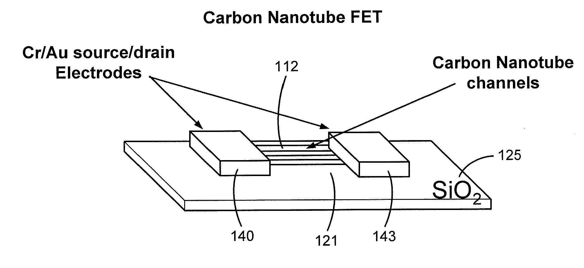
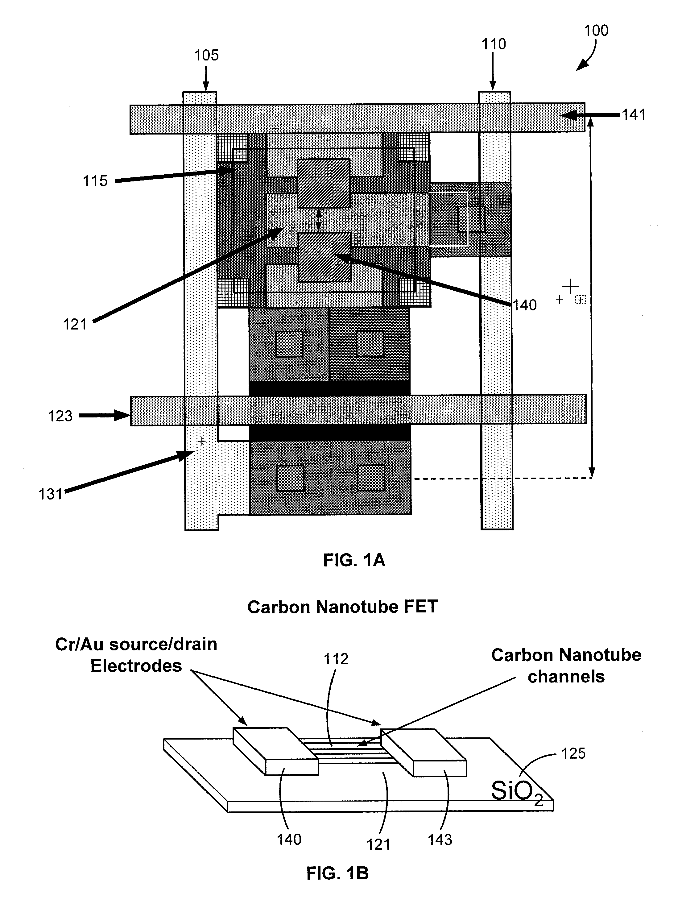
Hybrid sensor array

a sensor array and hybrid technology, applied in the field of hybrid sensor arrays, can solve the problems of not being able to demonstrate convincingly that the useful detection of specific analytes can be accomplished in this way, and no artificial system developed with such high dimensionality, and achieve the effects of high dimensionality, high dimensionality, and low cost of electronic chips

Inactive Publication Date: 2012-02-02
NANOSENSE
View PDF3 Cites 62 Cited by
  • Summary
  • Abstract
  • Description
  • Claims
  • Application Information

AI Technical Summary

Benefits of technology

[0008]The present invention provides a hybrid sensor array having high dimensionality fostering the selective detection of many different analyte categories. The system is fundamentally an array of digitally addressable carbon nanotube, nanowire, or graphene FET's, each of which is functionalized, that is made selectively responsive, by one or more interaction-mediating molecular species or hybrid molecular constructs, including but not limited to, single strand DNA or membrane proteins embedded in lipid carrier vehicles such as Nanodiscs. The inventive hybrid sensor arrays can be used in a variety of applications including the detection and identification of explosives, contraband, drug discovery, human outgas, medical applications, toxic industrial chemicals, agricultural organics, fugitive emissions and the like. Advantageously, the described class of hybrid sensor arrays combines the sensitivity of nanotube and other nanoscale transistor devices, the durability and potentially low cost of electronic chips and the high dimensionality required to discriminate amongst a large universe of potential analytes. When functionalized with membrane proteins for example, the inventive arrays of FETs allow interrogation of analyte interaction for use in the pharmaceutical industry such as for drug metabolism studies, pharmacokinetics, and metabolite toxicity analysis.

Problems solved by technology

Examples of covalent chemical attachment of biological molecules to nanotubes, including proteins and DNA, are known in the art, although it has not been convincingly demonstrated that useful detection of specific analytes can be accomplished in this way.
To date, no such artificial system has been developed which has such high dimensionality.

Method used


Image

  • Hybrid sensor array
  • Hybrid sensor array
  • Hybrid sensor array

Examples


examples

[0071]Example 1 illustrates certain electronic characteristics of one nanotube mat FET on a nanotube FET sensor chip.

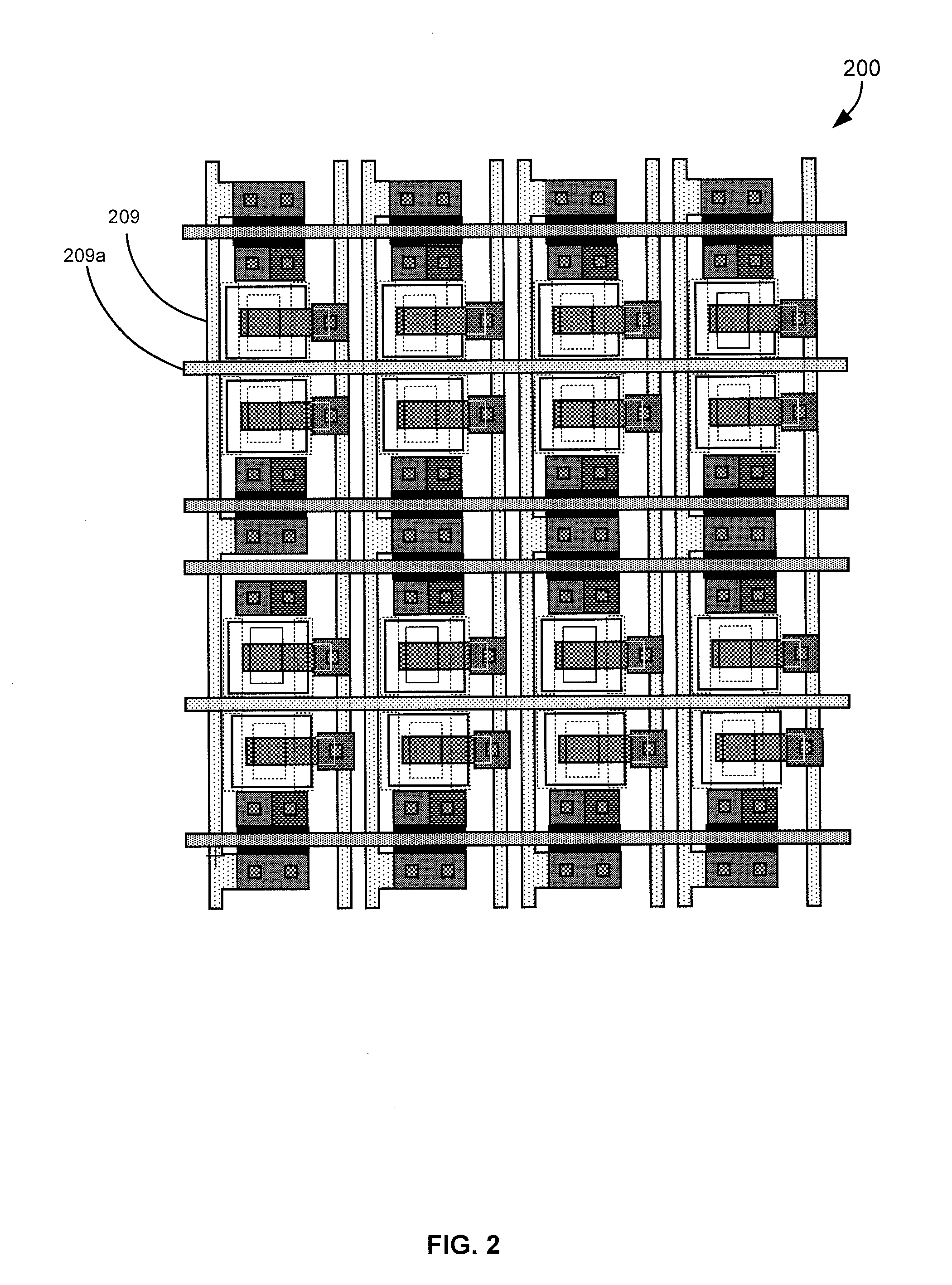
[0072]A hybrid sensor array was constructed containing 16 nanotube FETs along with a companion TFT in a 96-well sensor module and the attendant electronics to control gate voltage wherein each transistor is individually controllable and the source / drain voltage (common across the chip) and to read the current from each of the 1,536 sensor transistors. The 16 transistors in each well is identically functionalized, allowing the S / N benefit of averaging, while the 96 wells on each chip affords high dimensionality in this artificial “olfactory epithelium”. A single breadboard airpath contains 3 such chips in series, along with the attendant control electronics.

[0073]In FIG. 8, the data show the source / drain current (▪) across the range of gating voltages immediately after fabrication. The high current level and low on-to-off current ratio is indicative of a high metallic ...


PUM

PropertyMeasurementUnit
lengthaaaaaaaaaa
diameteraaaaaaaaaa
diameteraaaaaaaaaa

Abstract

The present invention provides devices, methods and systems to selectively detect the binding of a molecular species to a biomolecule. In its olfactory sensing application, the hybrid sensor arrays of the present invention provide a high dimensional signature of odorants present that is also readily reversible, together enabling the identification and localization of a source analyte in the presence of the background odorant landscape inherent in a real-world setting.

Description

CROSS-REFERENCE TO RELATED APPLICATIONS[0001]This application claims priority to U.S. Provisional Patent Application No. 61 / 290,859, filed Dec. 29, 2009, the disclosure of which is hereby incorporated by reference in its entirety for all purposes.BACKGROUND OF THE INVENTION[0002]Field effect transistors (FETs) fabricated from component semiconducting carbon nanotubes (NTs) have been studied extensively for their potential as sensors. A number of properties of these devices have been identified, and different mechanisms have been proposed to describe their sensing behavior. Devices that incorporate carbon nanotubes have been found to be sensitive to various gases, such as oxygen and ammonia, and these observations have confirmed the notion that such devices can operate as sensitive chemical sensors.[0003]U.S. Pat. No. 7,129,554 to Lieber, discloses electrical devices comprised of nanoscopic wires. The nanoscopic wires can be nanotubes, such as single-walled carbon nanotubes. They can...

Claims


Application Information

Patent Timeline
Patent Type & Authority Applications(United States)
IPC IPC(8): C40B30/04H01L29/775B82Y15/00B82Y99/00
CPCB82Y15/00G01M3/20G01N33/0031G01N27/4148G01N27/4141G01N27/4145G01N27/4146G01N33/54373G01N33/0047H10K10/484H10K19/10H10K85/225H01L29/786
Inventor RHODES, PAUL A.KHAMIS, SAMUEL M.
Owner NANOSENSE
Why Eureka
Try Eureka