Method and apparatus for AD conversion, semiconductor device for detecting distribution of physical quantity, and electronic apparatus

a technology of analog to digital and a/d, applied in the direction of single-carrier transmission of single-carrier television signals, instruments, television systems, etc., can solve the problems of noise, noise, power consumption, noise picked up by lines, etc., and avoid the problem of increasing noise level and power consumption. , the effect of minimizing the increase in the circuit area

Active Publication Date: 2005-09-22
SONY CORP
View PDF3 Cites 100 Cited by
  • Summary
  • Abstract
  • Description
  • Claims
  • Application Information

AI Technical Summary

Benefits of technology

[0093] The A/D converter is composed of the comparator and the counter in pair. When the unit signal outputted by the semiconductor device having an array of unit elements is to be processed, each of a plurality of A/D converters arranged in the direction of rows (the direction of an array of unit element columns) are provided with a counter. This arrangement eliminates the need for routing t

Problems solved by technology

The A/D conversion mechanisms disclosed in these documents have difficulty in terms of the size and area of a circuit, power consumption, the number of interfacing lines with another functional block, noise picked up by the lines, and current consumption.
Because of this routing, an increase in noise and an increase in power consumption become a concern.
An increase in noise and an increase in power consumption due to data transfer become a concern.
The

Method used


Image

  • Method and apparatus for AD conversion, semiconductor device for detecting distribution of physical quantity, and electronic apparatus
  • Method and apparatus for AD conversion, semiconductor device for detecting distribution of physical quantity, and electronic apparatus
  • Method and apparatus for AD conversion, semiconductor device for detecting distribution of physical quantity, and electronic apparatus

Examples


first embodiment

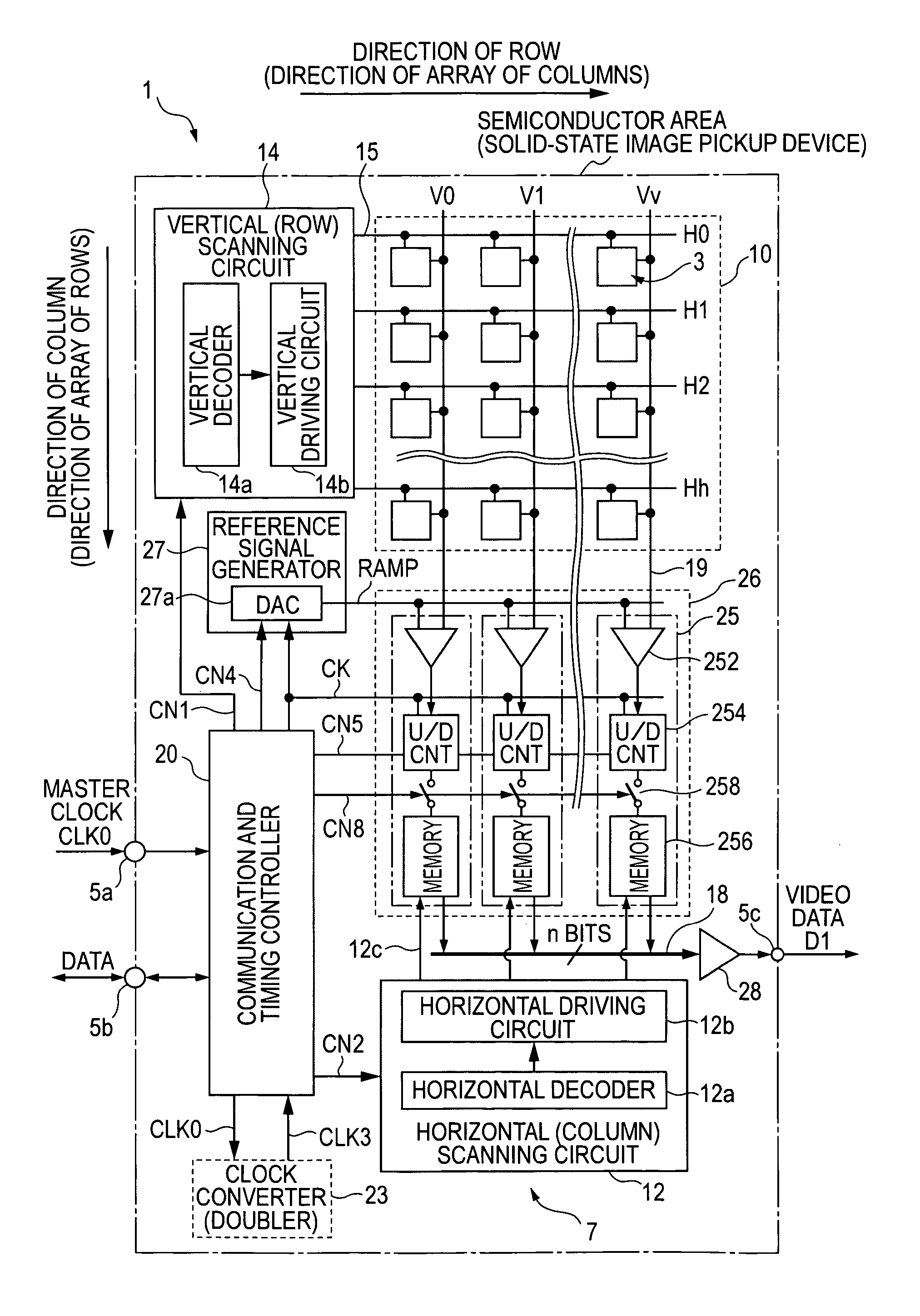
[0104]FIG. 1 illustrates a CMOS solid-state image pickup device (CMOS image sensor) 1 in accordance with the present invention. The CMOS solid-state image pickup device 1 is one example of an electronic apparatus of the present invention.

[0105] The solid-state image pickup device 1 includes a pixel section having a two-dimensional matrix of pixels, each pixel forming a light receiving element (as one example of a charge generator) that outputs a voltage signal responsive to an input amount of light, and correlated double sampling (CDS) units and analog-to-digital (A / D) converters arranged in a column parallel fashion.

[0106] The “arrangement in the column parallel fashion” means that a plurality of CDS units and a plurality of A / D converters are arranged in parallel with respective vertical signal lines 19. The plurality of these elements may be arranged on one edge of the columns of pixels in the pixel array 10 (i.e., on the output side at the lower side of the pixel array 10 as sh...

second embodiment

[0189] The column A / D converter 25 of the second embodiment includes a n-bit data memory 256, arranged in a subsequent stage to the counter 254, for storing the count result stored in the counter 254, and a switch 258 arranged between the counter 254 and the data memory 256.

[0190] The switches 258 are commonly supplied with a memory transfer command pulse CN8 as a control pulse at a predetermined timing by the communication and timing controller 20. Upon receiving the memory transfer command pulse CN8, the switch 258 transfers the count of the corresponding counter 254 to the data memory 256. The data memory 256 stores the incoming count.

[0191] The mechanism of storing the count of the counter 254 to the data memory 256 at a predetermined timing is not limited to the switch 258. For example, the counter 254 is directly connected to the data memory 256 and an output enable terminal of the counter 254 is controlled by the memory transfer command pulse CN8. Alternatively, the memory t...


PUM


Abstract

A column analog-to-digital converter having a voltage comparator and a counter is arranged for each a vertical signal line. The voltage comparator compares a pixel signal inputted via the vertical signal line at each row control signal line with a reference voltage, thereby generating a pulse signal having a length in time axis corresponding to the magnitude of a reset component and a signal component. The counter counts a clock to measure the width of the pulse signal until the end of the comparison operation of the comparator, and stores a count at the end of the comparison. A communication and timing controller controls the voltage comparator and the counter so that, in a first process, the voltage comparator performs a comparison operation on a reset component with the counter performing a down-counting operation, and so that, in a second process, the voltage controller performs the comparison operation on a signal component with the counter performing an up-counting operation.

Description

BACKGROUND OF THE INVENTION [0001] 1. Field of the Invention [0002] The present invention relates to an analog-to-digital (A / D) conversion method, an A / D converter, a semiconductor device, having a plurality of unit elements, for detecting a distribution of a physical quantity, and an electronic apparatus. In particular, the present invention relates to a technique for converting an analog output into digital data in a semiconductor device and an electronic apparatus, in which a plurality of unit elements responsive to an electromagnetic wave inputted from the outside, such as light or radiation rays, converts the input electromagnetic wave into the distribution of the physical quantity as an electrical signal, and the electrical signal is selectively read through address control. [0003] 2. Description of the Related Art [0004] Semiconductor devices for detecting a distribution of physical quantities are widely used. Such semiconductor device includes unit elements (such as pixels) ...

Claims


Application Information

Patent Timeline
IPC IPC(8): H03M1/10H03M1/12H03M1/56H04N5/335H04N5/355H04N5/357H04N5/363H04N5/378
CPCH03M1/1019H03M1/123H03M1/56H04N5/378H04N5/3575H04N5/363H04N5/335H04N25/00H04N25/616H04N25/65H04N25/75A01K85/00
Inventor MURAMATSU, YOSHINORIFUKUSHIMA, NORIYUKINITTA, YOSHIKAZUYASUI, YUKIHIRO
Owner SONY CORP
Why Eureka
Try Eureka