Heat spreader and semiconductor device and package using the same

a heat spreader and semiconductor technology, applied in semiconductor devices, semiconductor/solid-state device details, electrical devices, etc., can solve the problems of reducing the reliability of heat sink or radiating fin bonding in a face-down structure, nitride substrate, and reducing the power consumption of semiconductor devices. , to achieve the effect of high thermal conductivity, good air tightness, and large thermal conductivity

Inactive Publication Date: 2006-06-27
KOBE STEEL LTD
View PDF15 Cites 103 Cited by
  • Summary
  • Abstract
  • Description
  • Claims
  • Application Information

AI Technical Summary

Benefits of technology

[0026]As described above, each heat spreader according to the present invention is composed of a diamond layer, which has an extremely high thermal conductivity, and one or two metal or ceramic members, which have a large thermal conductivity. Therefore, the heat spreaders have a thermal conductivity, across the thickness, equal to or more than that of a composite material of copper and tungsten or that of aluminum nitride, both of which have been used for heat spreaders. In addition, the heat spreaders have good air-tightness and are not warped or cracked. Furthermore, the heat spreaders, having a nearly equivalent thermal expansion coefficient, across the plane, to that of

Problems solved by technology

When a metal radiating fin is bonded entirely on the top surface of such a large aluminum nitride substrate, the aluminum nitride substrate may cause defects such as cracking during heat cycles due to the difference in thermal expansion coefficients between the aluminum nitride substrate and the metal radiating fin.
Nevertheless, these semiconductor packages have difficulty in meeting a further increase in the power-consumption of the semiconductor devices

Method used


Image

  • Heat spreader and semiconductor device and package using the same
  • Heat spreader and semiconductor device and package using the same
  • Heat spreader and semiconductor device and package using the same

Examples


example 1

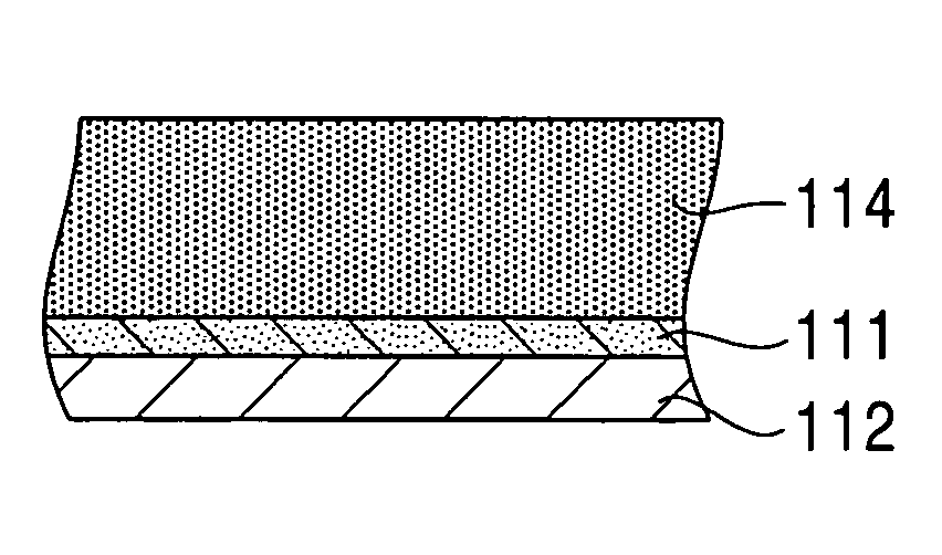
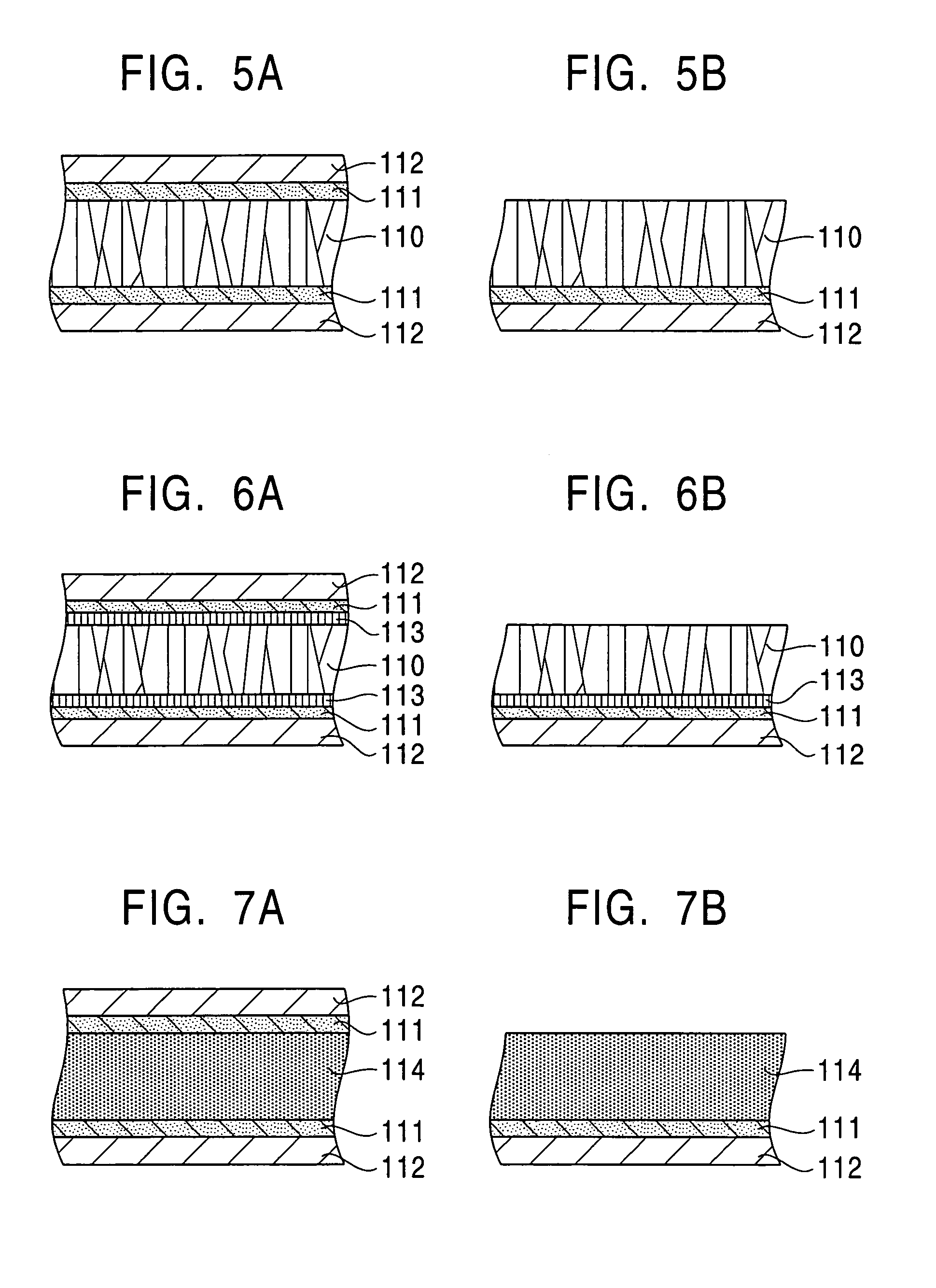
[0076]A diamond layer having a thermal conductivity of 800 W / (m·K) or more was formed on the reverse surface of a silicon wafer by CVD. This diamond layer, which was a microcrystal having a thickness of 0.05 mm, was notched in advance to make the diamond layer discontinuous. These notches suppress warpage of the wafer and facilitate division of the wafer into chips. Then, semiconductor devices were prepared on a surface of the silicon wafer facing away from the diamond layer. Semiconductor chips with a diamond heat spreader were prepared from this silicon wafer. These chips had an external size of 23 mm by 25 mm and a power consumption of 70 W.

example 2

[0077]Resin wiring substrates were prepared with a liquid crystal polymer as a base resin. The resin wiring substrates each had copper foils thermally compressed on both surfaces. One of these copper foils was etched to form a wiring layer having a pattern, and was then coated with an insulating resin. The semiconductor chips prepared in Example 1 were mounted on the resin wiring substrates by wire bonding to form semiconductor packages having a face-down structure. The semiconductor chips each had 478 pins in the semiconductor packages.

[0078]The semiconductor chips in the present invention are not limited to ball grid array (BGA) packages and may be applied to various packages.

example 3

[0079]Ten samples were selected from the semiconductor packages prepared in Example 2. Each heat spreader in these samples was partially coated with aluminum having a thickness of 100 nm to equip the heat spreader with an aluminum radiating fin having an external size of 35 mm by 39 mm. On the other hand, ten additional samples were selected from the semiconductor packages prepared in Example 2. Each heat spreader in these samples was coated with a polymer adhesive on its ciliary surface to equip the heat spreader with the aluminum radiating fin. A heat cycle test was performed on both samples. This test was continued for 500 cycles of −40° C., room temperature, and 110° C. This test showed that the heat spreaders in both samples did not develop cracks or other defects.


PUM


Abstract

A semiconductor device and package has a heat spreader directly disposed on the reverse surface of the semiconductor device. This heat spreader includes a diamond layer or a layer containing diamond and ceramics such as silicon carbide and aluminum nitride. The heat spreader is directly formed on a substrate for the semiconductor device. In particular, the heat spreader is composed of a diamond layer and one or two metal or ceramic members, which are bonded to the diamond layer with one or two polymer adhesive layers. This diamond layer has a fiber structure across the thickness or a microcrystalline structure. Cilia are formed on a surface of the diamond layer facing the one or two metal or ceramic members.

Description

BACKGROUND OF THE INVENTION[0001]1. Field of the Invention[0002]The present invention relates to heat spreaders for semiconductor devices to prevent a temperature rise due to heat generated by the semiconductor devices. In addition, the present invention relates to semiconductor devices and packages with the heat spreaders.[0003]2. Description of the Related Art[0004]To facilitate heat dissipation from semiconductor devices, for example, a semiconductor package with a combination of a high thermal-conductivity ceramic base material and a resin wiring substrate such as a printed circuit board has been proposed in Japanese Unexamined Patent Application Publication No. 10-275879. This semiconductor package includes a semiconductor device mounted on the bottom surface of an aluminum nitride heat spreader and a resin wiring substrate bonded around the semiconductor device. This resin wiring substrate has a wiring layer wired to a signal wiring of the semiconductor device. Semiconductor p...

Claims


Application Information

Patent Timeline
IPC IPC(8): H01L29/06H01L23/06H01L23/10H01L23/495H01L23/373
CPCH01L23/3732H01L2924/12044H01L2924/0002H01L2924/00
Inventor TACHIBANA, TAKESHIHAYASHI, KAZUSHIINOUE, KENICHIYOKOTA, YOSHIHIROKOBASHI, KOJIKAWAKAMI, NOBUYUKIKOBORI, TAKASHI
Owner KOBE STEEL LTD
Why Eureka
Try Eureka