Force sensitive touch sensor

a touch sensor and force technology, applied in the field of sensors, can solve the problems of brittleness and cracking, furthermore expensive, and disturb the clean design of the front side of the consumer product, and achieve the effect of widening the tolerance and more accurate force measuremen

Active Publication Date: 2016-08-16
SONY CORP
View PDF14 Cites 10 Cited by
  • Summary
  • Abstract
  • Description
  • Claims
  • Application Information

AI Technical Summary

Benefits of technology

[0007]According to an aspect of the present invention, a sensor comprising an insulating support layer and an electrically conductive sensor structure is provided. The electrically conductive sensor structure comprises a piezoresistive material and is configured to provide the resistance varying in response to a force being applied to the insulating support layer. The piezoresistive material comprises graphene. Graphene is an electrically conductive material and is extremely durable. Furthermore, as graphene is based on carbon, no expensive raw material is needed for producing graphene. Graphene is essentially an isolated atomic plane of graphite. Moreover, graphene is a very strong material, even stronger than diamond. It provides a very good heat transfer and a very high electric conductance, one million times higher than copper. Furthermore, due to the isolated atomic plane, it is very thin and at the same time more elastic than a crystalline material. At the same time graphene provides a high transparency or opacity, for example, an atomic monolayer absorbs only 2.3 percent of white light. Graphene has furthermore piezoresistive properties. This allows to create very sensitive force sensors and sensor dimensions can be made very small with the same performance compared to conventional sensors, for example sensors based on indium tin oxide. The low resistance of graphene may significantly lower the noise of the sensor compared to other types of strain gauge sensors. Therefore, by using graphene in the above-described force sensor a more robust sensor can be provided and cost and space may be saved.
[0009]According to another embodiment, the electrically conductive sensor structure is further configured to provide an electrical property varying in response to light incidence on the graphene. For example, the electrically conductive sensor structure may comprise a metal-graphene-metal photo detector allowing an efficient photo detection. Due to the band structure of graphene, a photoresponsivity may be achieved. Therefore, an electrical property of the electrically conductive sensor structure may vary in response to light incidence on the graphene, for example an electrical current may be generated by the graphene or by the metal-graphene-metal arrangement in response to light incidence. Therefore, a photosensitive sensor may be integrated into the force sensor and may simplify a mechanical design of for example a mobile phone. Furthermore, a cleaned-up design of a front surface of the mobile phone may be achieved.
[0012]According to another aspect of the present invention, a display comprising the sensor described above is provided. The insulating support layer comprises a window layer of the display. Furthermore, the insulating support layer may comprise a flexible layer arranged below the window layer of the display. Due to the transparency of the graphene, the sensor may be arranged in an upper side of a display, for example a liquid crystal display (LCD), without disturbing an optical output of the display.
[0014]According to a further embodiment, for calibrating the sensor, a plurality of touches are performed and corresponding resistances are measured. Each touch has a predetermined force at a predetermined touch position. The measured resistances and the associated predetermined forces and predetermined touch positions are e.g. stored in a calibration matrix or in another way calibrated, e.g. by an algorithm. Then, the touch force of the user touching the sensor is determined based on the determined resistance and touch position in connection with the calibration matrix. This may provide a more accurate force measurement based on the fact that it is known where the force is applied on the insulating support layer due to the capacitively sensored touch position. Depending on the needed accuracy, the calibration matrix may be setup for each individual sensor separately and stored for example in a driver circuit controlling the sensor. If a wider tolerance is acceptable, the calibration matrix may be setup once for all sensors.
[0016]According to the further embodiment, the above-described sensor may be used to determine a distance to an object in an environment of the sensor. Therefore, predetermined infrared light is emitted to the object by an infrared transmitter. Infrared light reflected from the object is received by the electrically conductive sensor structure, and the distance to the object is determined based on the received infrared light. A distance measuring based on infrared light is known in the art and will therefore not be described in more detail here. In combination with an infrared transmitter, for example an infrared light emitting diode (LED) or a backlight illumination of a display, a distance measuring may be realized which may be integrated at low cost in for example a mobile phone without disturbing a clean design of a front side of the phone. The infrared transmitter may be arranged below the sensor and may transmit the infrared light through the sensor due to the transparency of graphene.
[0020]According to another aspect of the present invention, a touch sensitive user interface is provided. The touch sensitive user interface comprises the above-described sensor and a processing unit coupled to the electrically conductive sensor structure of the sensor. The processing unit is adapted to determine a force being applied by a user touching the sensor based on the varying resistance. The processing unit may furthermore be adapted to perform any one of the above-described methods. Therefore, a touch sensitive user interface is enabled for inputting comprehensive and complex control information in an easy and intuitive way. Furthermore, the touch sensitive user interface is robust and does not comprise expensive materials.

Problems solved by technology

However, it may be brittle and may crack and is furthermore expensive due to the cost of indium.
This may disturb a clean design of the front side of the consumer product, especially when these components are to be integrated in a mobile phone.

Method used


Image

  • Force sensitive touch sensor
  • Force sensitive touch sensor
  • Force sensitive touch sensor

Examples


Embodiment Construction

[0028]In the following, exemplary embodiments of the present invention will be described in more detail. It has to be understood that the following description is given only for the purpose of illustrating the principles of the invention and is not be taken in a limiting sense. Rather, the scope of the invention is defined only by the appended claims and is not intended to be limited by the exemplary embodiments hereinafter.

[0029]It is to be understood that the features of the various exemplary embodiments described herein may be combined with each other unless specifically noted otherwise. Same reference signs in the various drawings and the following description refer to similar or identical components.

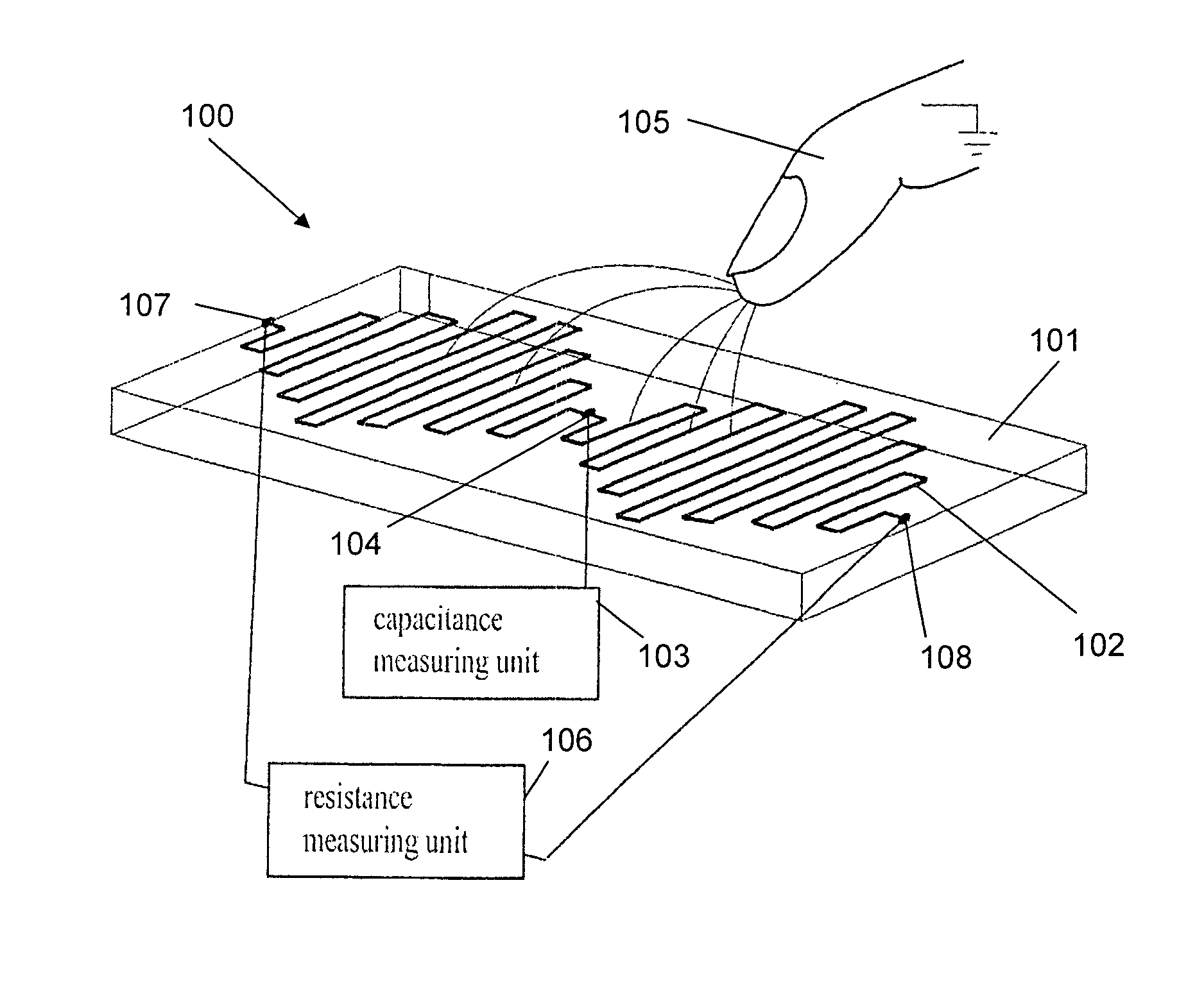
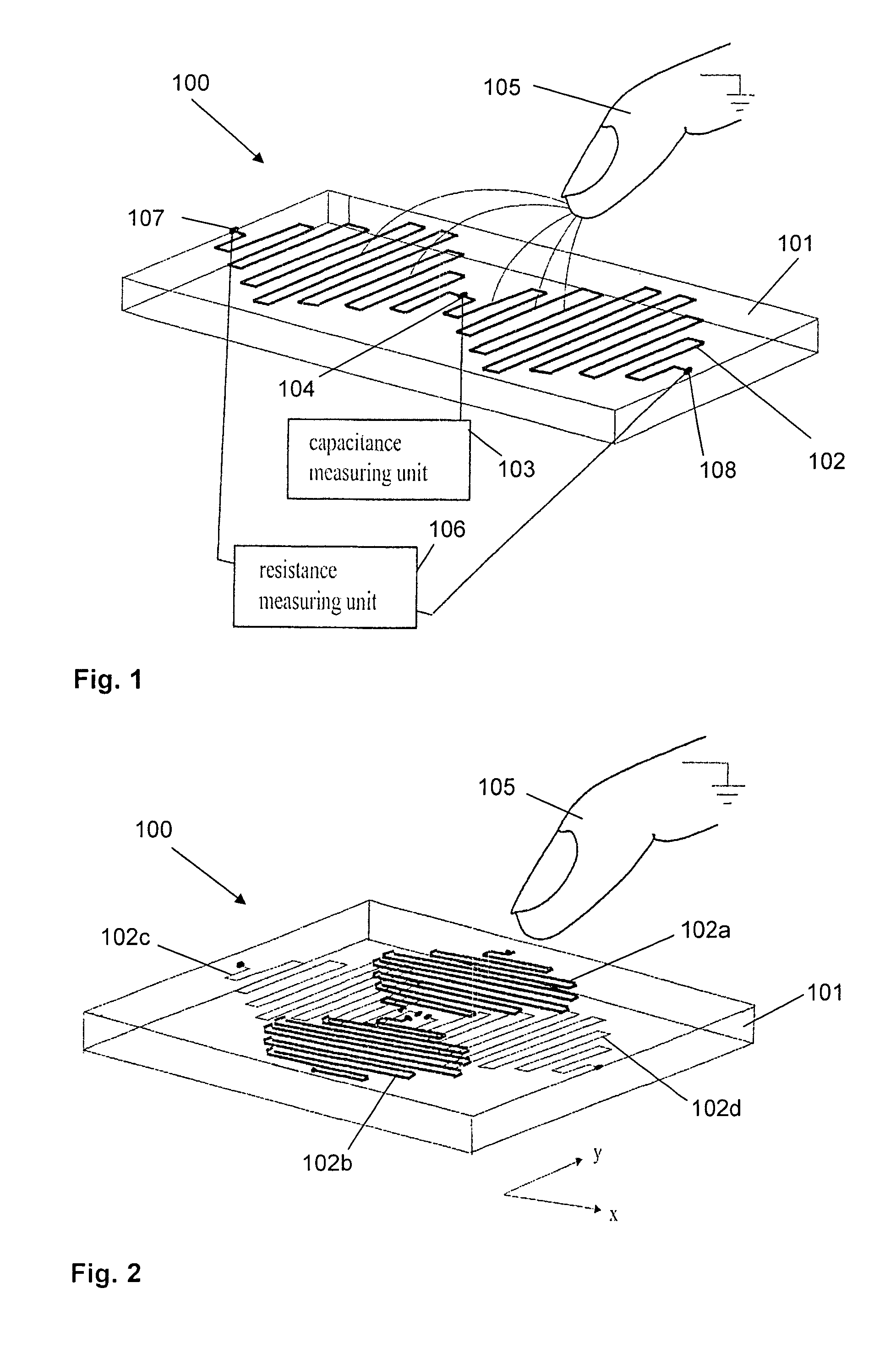
[0030]FIG. 1 shows a sensor 100 comprising an insulating support layer 101 and an electrically conductive sensor structure 102. The electrically conductive sensor structure 102 is arranged on an upper side of the insulating support layer 101. The electrically conductive sensor struc...


PUM

PropertyMeasurementUnit
transparencyaaaaaaaaaa
operational wavelength rangeaaaaaaaaaa
electrically conductiveaaaaaaaaaa

Abstract

A force sensitive touch sensor (100) is provided. The sensor (100) comprises an insulating support layer (101) and an electrically conductive sensor structure (102). The electrically conductive sensor structure (102) comprises a piezoresistive material and is configured to provide a resistance varying in response to a force being applied to the insulating support layer (101). The piezoresistive material comprises graphene.

Description

FIELD OF THE INVENTION[0001]The present application relates to a sensor comprising an insulating support layer and an electrically conductive sensor structure which is configured to provide a resistance varying in response to a force applied to the sensor. The present application relates especially to a sensor in which the electrically conductive sensor structure comprises a graphene. The present application relates furthermore to a display and a touch sensitive user interface comprising the force sensitive touch sensor and to a device comprising the touch sensitive user interface. Finally, the present application relates to methods for operating the force sensitive touch sensor.BACKGROUND OF THE INVENTION[0002]Touch sensors are known in the art for controlling devices via a user interface or a man machine interface. Traditionally, touch sensors are adapted to detect a touch position in a two-dimensional way. Especially consumer products, for example mobile telephones, mobile naviga...

Claims


Application Information

Patent Timeline
Patent Type & Authority Patents(United States)
IPC IPC(8): G01L1/04G01L1/18G06F3/041G06F3/044G06F3/042G01L1/14
CPCG06F3/041G06F3/0414G06F3/0421G06F3/044G01L1/14G01L1/18G06F3/0443G06F3/0445
Inventor ANG.BERG, PETERKLINGHULT, GUNNAR
Owner SONY CORP
Why Eureka
Try Eureka