Vertical transistor fabrication and devices

a technology of vertical fins and transistors, applied in the direction of transistors, semiconductor devices, electrical equipment, etc., can solve the problems of difficult forming of individual components and electrical contacts

Active Publication Date: 2016-08-30
IBM CORP
View PDF9 Cites 57 Cited by
  • Summary
  • Abstract
  • Description
  • Claims
  • Application Information

AI Technical Summary

Benefits of technology

[0007]A method of fabricating a vertical field effect transistor includes forming a first recess in a substrate, wherein the first recess has a first bottom surface; epitaxially growing a first drain from the first bottom surface of the first recess; epitaxially growing a second drain from the second bottom surface of a second recess formed in the substrate; epitaxially growing a channel material on the first drain and the second drain; forming troughs in the channel material to form one or more fin channels on the first drain and one or more fin channels on the second drain, wherein the troughs over the first drain extend to the surface of the first drain, and the troughs over the second drain extend to the surface of the second drain; forming a gate structure on each of the one or more fin channels; and growing sources on each of the fin channels associated with the first and second drains.
[0008]A vertical field effect transistor includes a first recess in a substrate, wherein the first recess has a first bottom surface. A first drain is grown from the first bottom surface of the first recess, wherein the first drain has the same crystal orientation as the first bottom surface. A second recess is formed in the substrate, wherein the second recess has a second bottom surface, and a second drain is grown on the second bottom surface of a second recess formed in the substrate, wherein the second drain has the same crystal orientation as the second bottom surface. One or more fin channels are formed on the first drain, wherein the one or more fin channels on the first drain have the same crystal orientation as the first bottom surface, and one or more fin channels are formed on the second drain, wherein the one or more fin channels on the second drain have the same crystal orientation as the second bottom surface. A gate structure is formed on each of the fin channels, and sources are grown on each of the fin channels associated with the first drain and the second drain, wherein the sources have the same crystal orientation as the fin channels.

Problems solved by technology

With ever decreasing device dimensions, forming the individual components and electrical contacts become more difficult.

Method used


Image

  • Vertical transistor fabrication and devices
  • Vertical transistor fabrication and devices
  • Vertical transistor fabrication and devices

Examples


Embodiment Construction

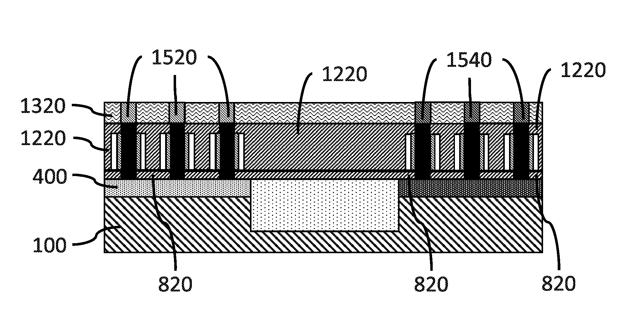
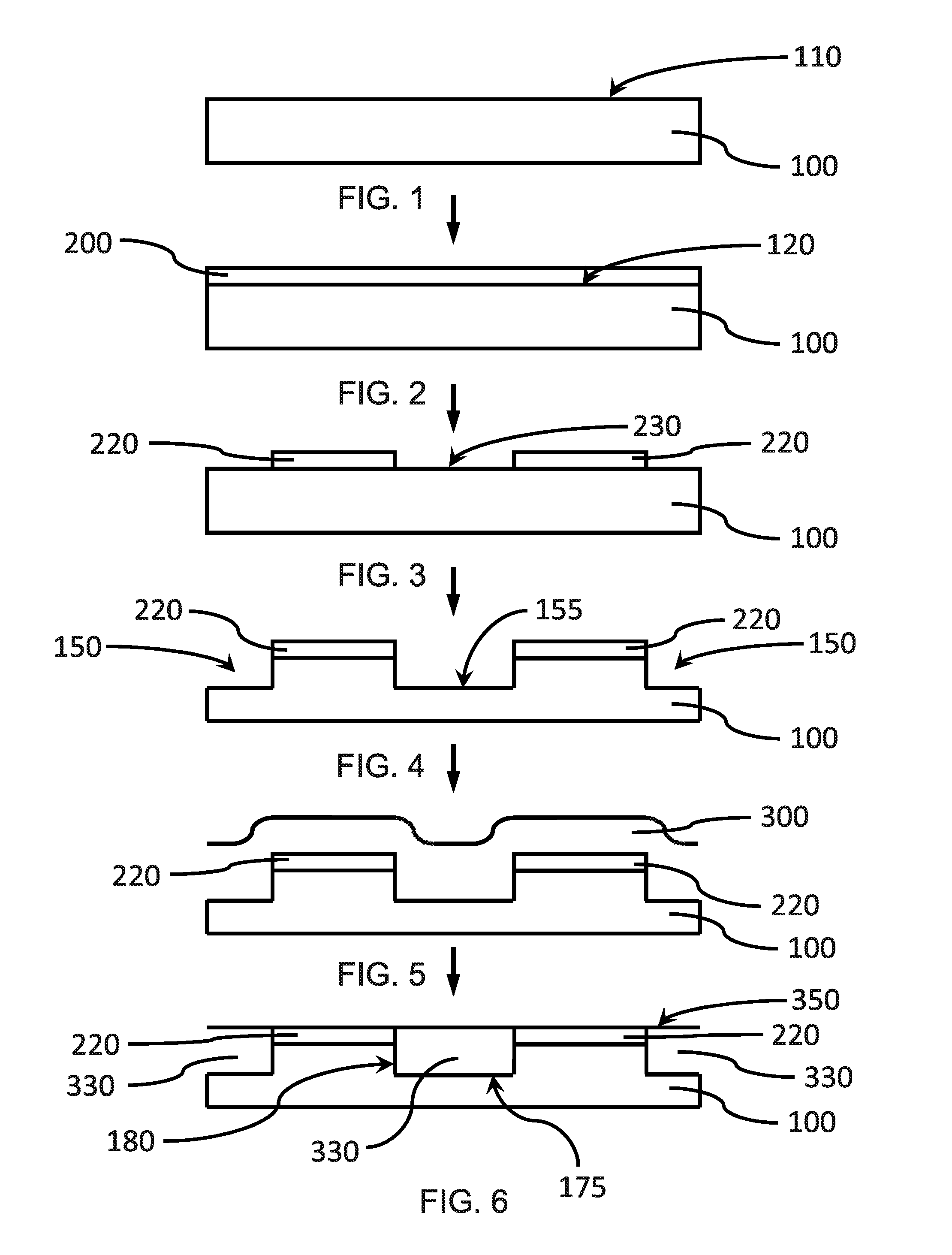
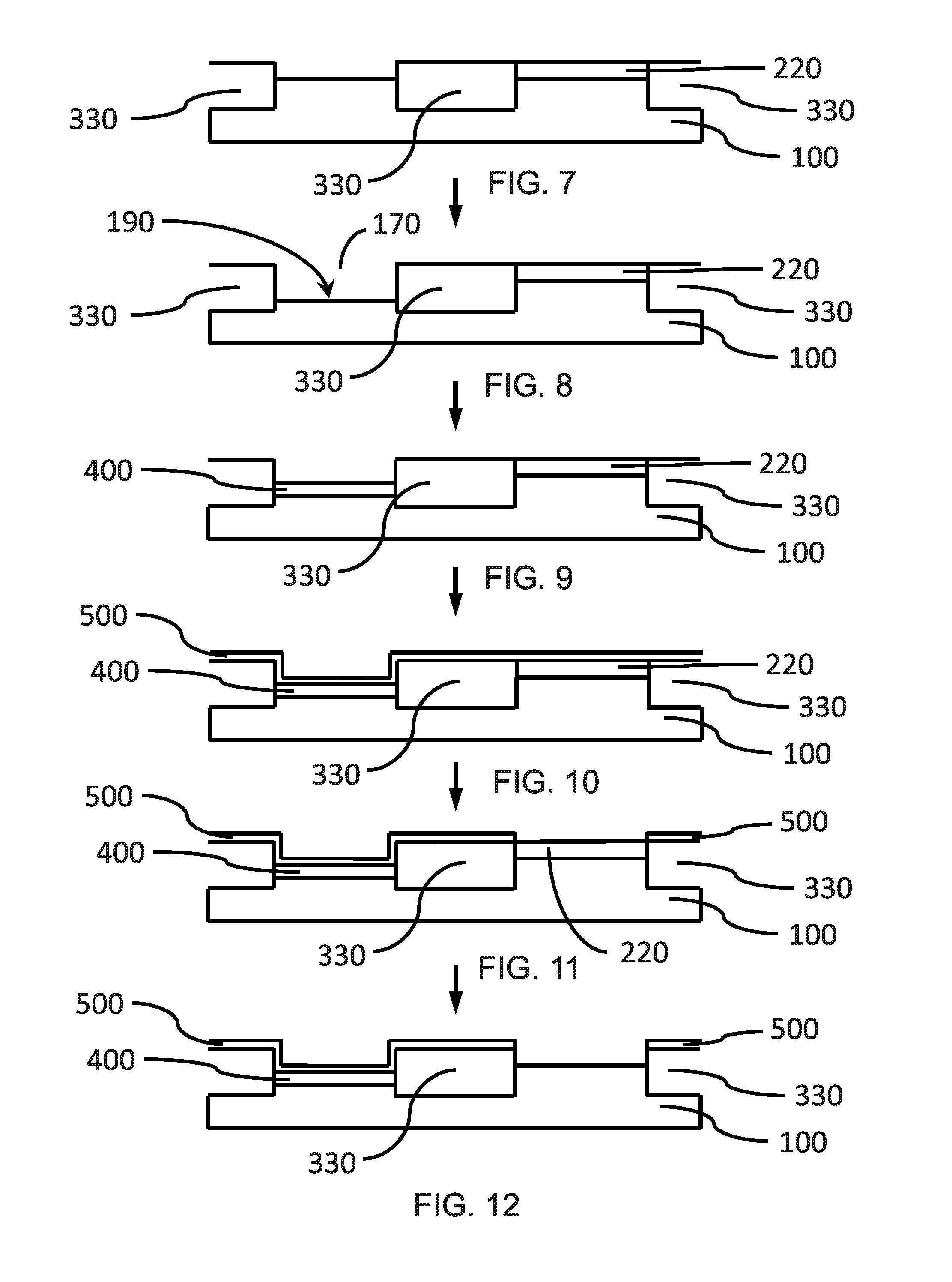
[0064]Principle and embodiments of the present disclosure relate to a semiconductor device structure with conductive elements stacked on the substrate to form a conductive path normal to the surface of the substrate on which the semiconductor structure is formed. An embodiment relates generally to a vertical finFET structure that provides enhanced geometries for electrical contact formation and current carrying properties. In an embodiment, a finFET semiconductor device has the drain, fin channel, and source device components arranged perpendicular to the plane of the substrate surface, which is referred to as a vertical stack. A vertically stacked finFET can have a longer gate length (i.e., height) and larger dielectric spacer than a horizontal (i.e., having the drain, fin channel, and source device components arranged parallel with the plane of the substrate surface) finFET having comparable contact gate pitch.

[0065]In one or more embodiments, a source, drain, and channel of a fin...


PUM


Abstract

A method of fabricating a vertical field effect transistor including forming a first recess in a substrate; epitaxially growing a first drain from the first bottom surface of the first recess; epitaxially growing a second drain from the second bottom surface of a second recess formed in the substrate; growing a channel material epitaxially on the first drain and the second drain; forming troughs in the channel material to form one or more fin channels on the first drain and one or more fin channels on the second drain, wherein the troughs over the first drain extend to the surface of the first drain, and the troughs over the second drain extend to the surface of the second drain; forming a gate structure on each of the one or more fin channels; and growing sources on each of the fin channels associated with the first and second drains.

Description

BACKGROUND[0001]1. Technical Field[0002]The present invention relates to methods of forming vertical finFET devices and the electronic device structures produced thereby, and more particularly to a method of epitaxially forming the drain, channel, and source of a vertical finFET such that the drain, channel, and source have the same crystal orientation.[0003]2. Description of the Related Art[0004]A Field Effect Transistor (FET) typically has a source, a channel, and a drain, where current flows from the source to the drain, and a gate that controls the flow of current through the channel. Field Effect Transistors (FETs) can have a variety of different structures, for example, FETs have been formed with the source, channel, and drain formed in the substrate material itself, where the current flows horizontally (i.e., in the plane of the substrate), and FinFETs have been formed with the channel extending outward from the substrate, but where the current also flows horizontally. The ch...

Claims


Application Information

Patent Timeline
Patent Type & Authority Patents(United States)
IPC IPC(8): H01L27/092H01L21/8238H01L29/786H01L29/78H01L29/423H01L27/112H01L29/66
CPCH01L21/823885H01L21/823814H01L21/823807H01L29/78618H01L29/78696H01L29/78642H01L29/78684H01L29/7848H01L29/42392H01L27/092H01L27/11273H01L29/66666H01L29/7827H01L29/7802H01L21/823871H01L21/823878H01L29/0847H01L29/167H10B20/40H01L21/823842H01L29/0653H01L29/1608H01L29/161H01L29/4966H01L29/045H01L29/0676H01L29/66439
Inventor ANDERSON, BRENT A.DORIS, BRUCE B.KIM, SEONG-DONGVENIGALLA, RAJASEKHAR
Owner IBM CORP
Why Eureka
Try Eureka