Vertical transistor having an asymmetric gate

a technology of vertical transistors and transistors, applied in the field of vertical transistor devices with asymmetric gates, can solve the problem of difficult fabrication of lateral structures of asymmetric transistor devices

Inactive Publication Date: 2013-04-18
IBM CORP
View PDF7 Cites 46 Cited by
  • Summary
  • Abstract
  • Description
  • Claims
  • Application Information

AI Technical Summary

Problems solved by technology

However, it is difficult to fabricate an asymmetric transistor device to have a lateral structure where the gate characteristics vary in a manner that is parallel to the underlying channel.

Method used


Image

  • Vertical transistor having an asymmetric gate
  • Vertical transistor having an asymmetric gate
  • Vertical transistor having an asymmetric gate

Examples


Embodiment Construction

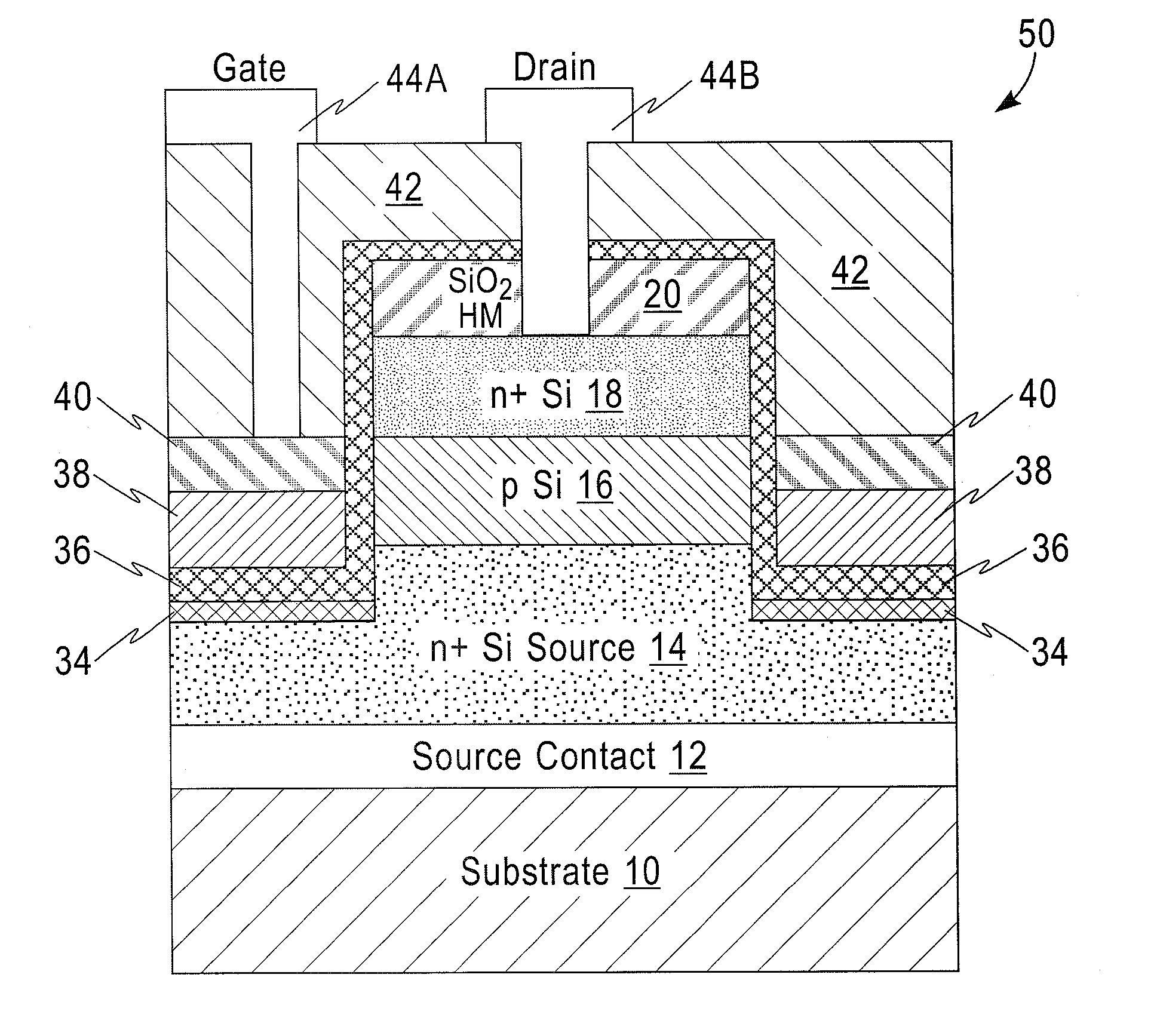
[0021]An important parameter of a MOSFET device is the effective work function (Φeff) of the gate, which is in contact with the gate dielectric. The Φeff affects the device flatband voltage (Vfb) and thus controls the threshold voltage (Vt) of the MOSFET.

[0022]FIGS. 1-12 show the fabrication of an asymmetric gate, vertical channel transistor device, specifically an nFET 50, in accordance with exemplary embodiments of this invention.

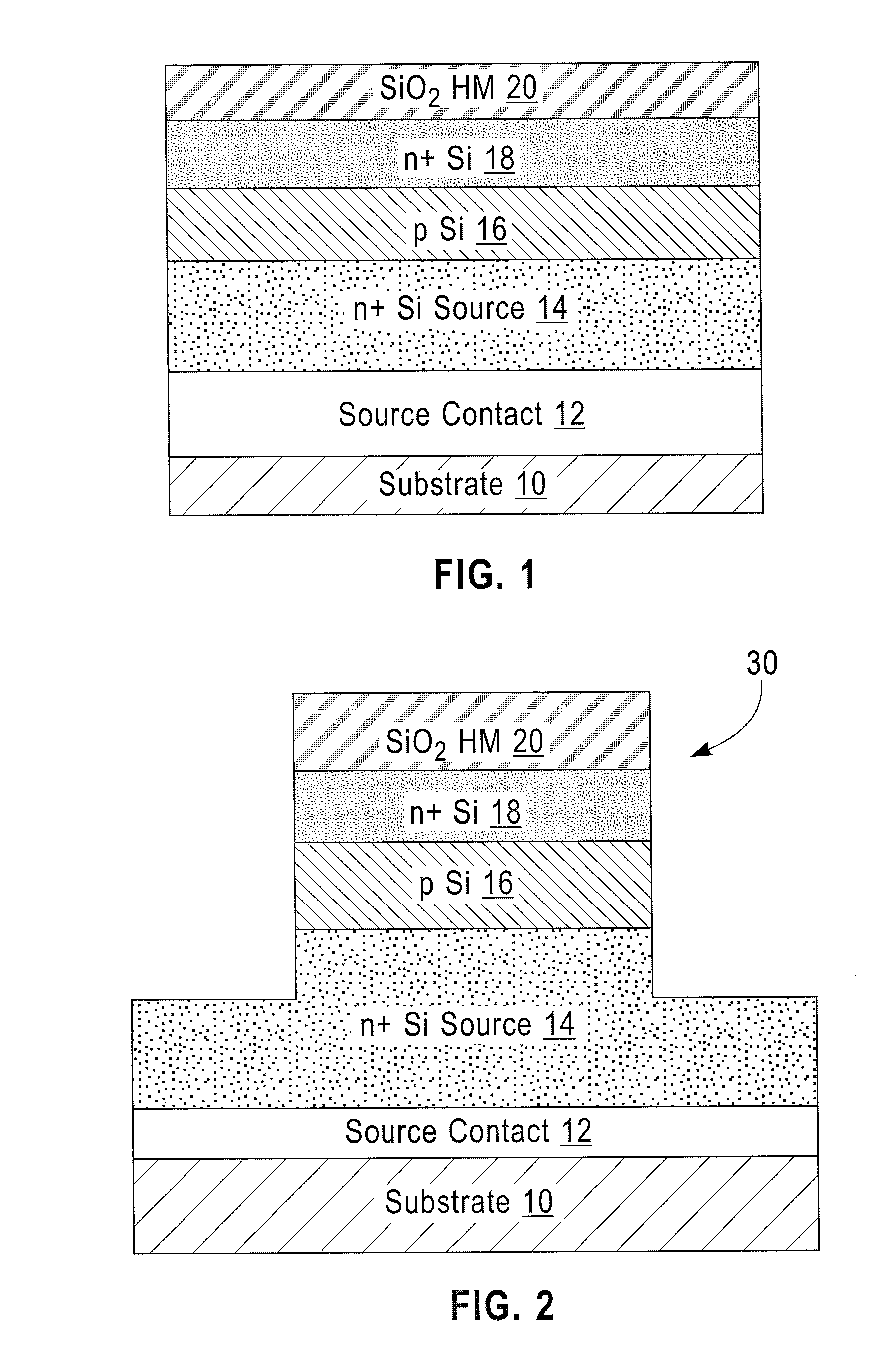
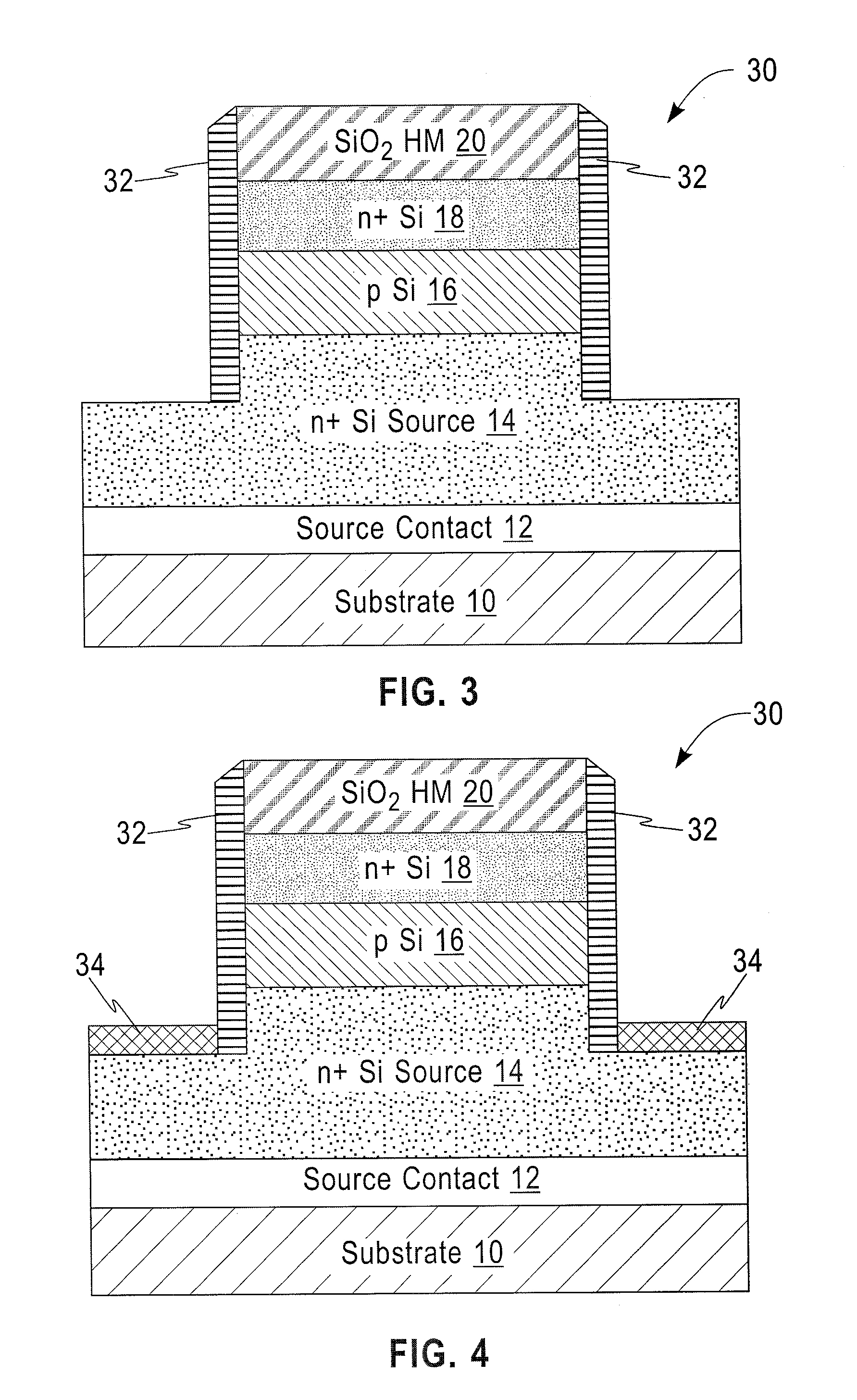
[0023]Referring to FIG. 1, an exemplary semiconductor structure according to the present invention comprises a semiconductor substrate 10 and a stack of material layers formed thereupon. The semiconductor substrate 10 has a semiconductor material, which may be selected from, but is not limited to, silicon, germanium, silicon-germanium alloy, silicon carbon alloy, silicon-germanium-carbon alloy, gallium arsenide, indium arsenide, indium phosphide, III-V compound semiconductor materials, II-VI compound semiconductor materials, organic semiconductor material...


PUM


Abstract

A transistor structure is formed to include a substrate and, overlying the substrate, a source; a drain; and a channel disposed vertically between the source and the drain. The channel is coupled to a gate conductor that surrounds the channel via a layer of gate dielectric material that surrounds the channel. The gate conductor is composed of a first electrically conductive material having a first work function that surrounds a first portion of a length of the channel and a second electrically conductive material having a second work function that surrounds a second portion of the length of the channel. A method to fabricate the transistor structure is also disclosed. The transistor structure can be characterized as being a vertical field effect transistor having an asymmetric gate.

Description

CROSS-REFERENCE TO A RELATED PATENT APPLICATION[0001]This patent application is a continuation application of copending U.S. patent application Ser. No. 13 / 271,812, filed Oct. 12, 2011, the disclosure of which is incorporated by reference herein in its entirety.TECHNICAL FIELD[0002]The exemplary embodiments of this invention relate generally to transistor devices and, more specifically, relate to asymmetric gate vertical transistor devices and to methods of fabricating same.BACKGROUND[0003]An asymmetric transistor device can provide enhanced current handling and increase output resistance. However, it is difficult to fabricate an asymmetric transistor device to have a lateral structure where the gate characteristics vary in a manner that is parallel to the underlying channel.[0004]Various vertical channel transistor devices have been previously proposed. For example, reference can be made to IEEE TRANSACTIONS ON ELECTRON DEVICES, VOL. 53, NO. 5, MAY 2006, Asymmetric Gate-Induced Dra...

Claims


Application Information

Patent Timeline
Patent Type & Authority Applications(United States)
IPC IPC(8): H01L21/336
CPCH01L29/4983H01L29/7827H01L29/78H01L29/66666H01L21/823885H01L21/823487
Inventor GUO, DECHAOHAN, SHU-JENWONG, KEITH KWONG HONYUAN, JUN
Owner IBM CORP
Why Eureka
Try Eureka