Super self-aligned BJT with base shorted field plate and method of fabricating

a bjt and base technology, applied in the direction of basic electric elements, electrical equipment, semiconductor devices, etc., can solve the problems of not revealing the practical structure or fabrication method of bjt devices for realizing the concept, increasing the resistance of collector series, and substantially increasing the peak fsub>t/sub>, so as to improve the breakdown/ron ratio and the ft*bvcbo product. , the effect of improving the produ

Active Publication Date: 2006-11-07
NAT SEMICON CORP
View PDF1 Cites 46 Cited by
  • Summary
  • Abstract
  • Description
  • Claims
  • Application Information

AI Technical Summary

Benefits of technology

[0009]The present invention provides a bipolar junction transistor (BJT) structure, and a method for fabricating the structure, in which a doped polysilicon filled trench is utilized to form both the extrinisic base contact region and a vertical field plate. A sacrificial mandrel of dielectric material is formed over regions that will become the BJT active area. This allows the poysilicon filled trench to be extended a...

Problems solved by technology

While the Hueting et al. publication provides a theoretical concept for improving the performance characteristics of a BJT device, it does not disclose a practical BJT device structure or fabrication method ...

Method used


Image

  • Super self-aligned BJT with base shorted field plate and method of fabricating
  • Super self-aligned BJT with base shorted field plate and method of fabricating
  • Super self-aligned BJT with base shorted field plate and method of fabricating

Examples


Embodiment Construction

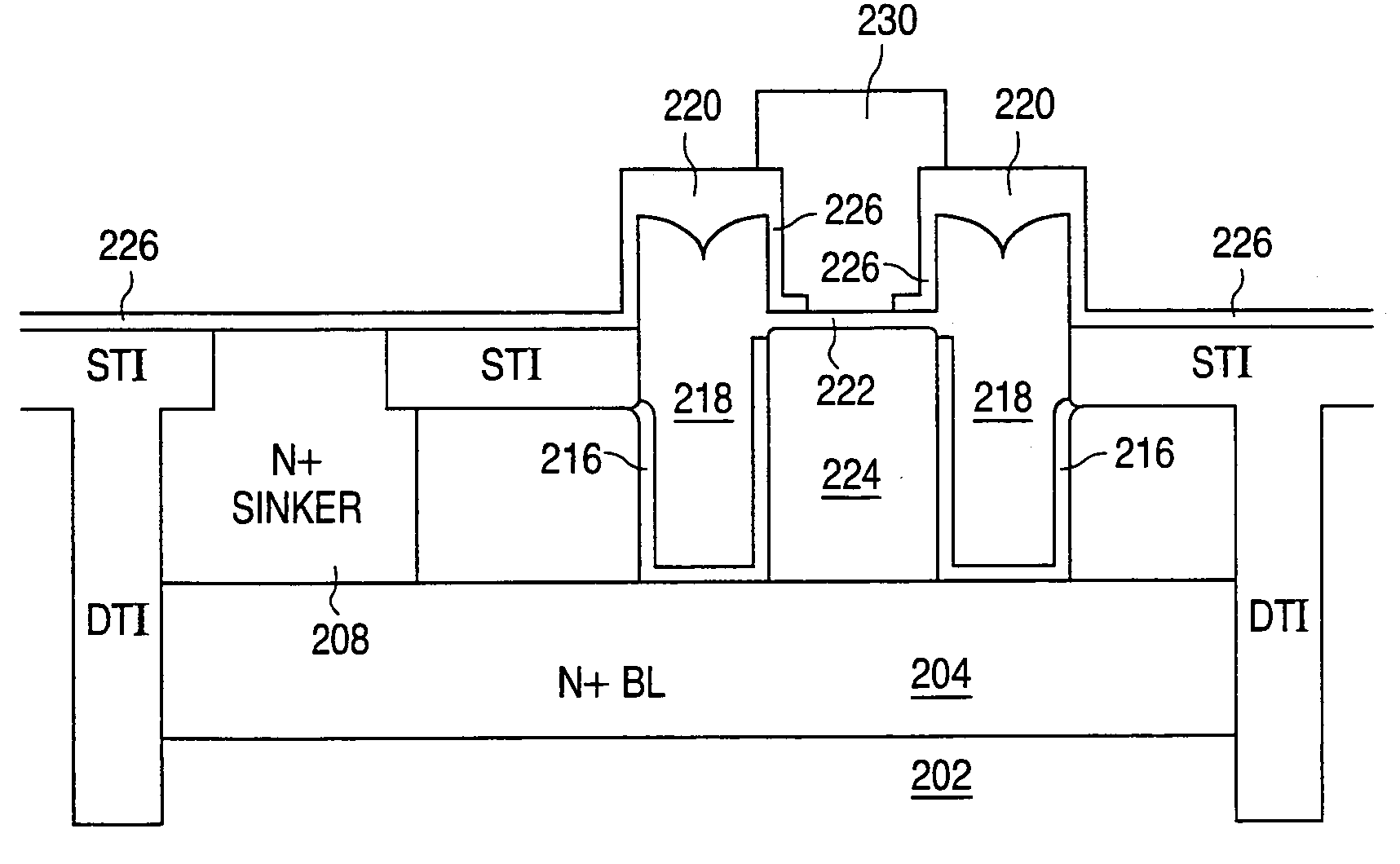
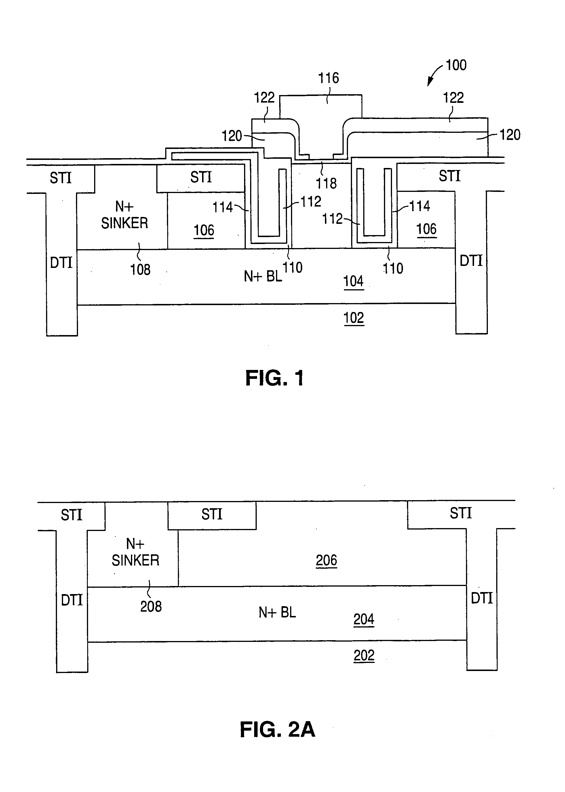
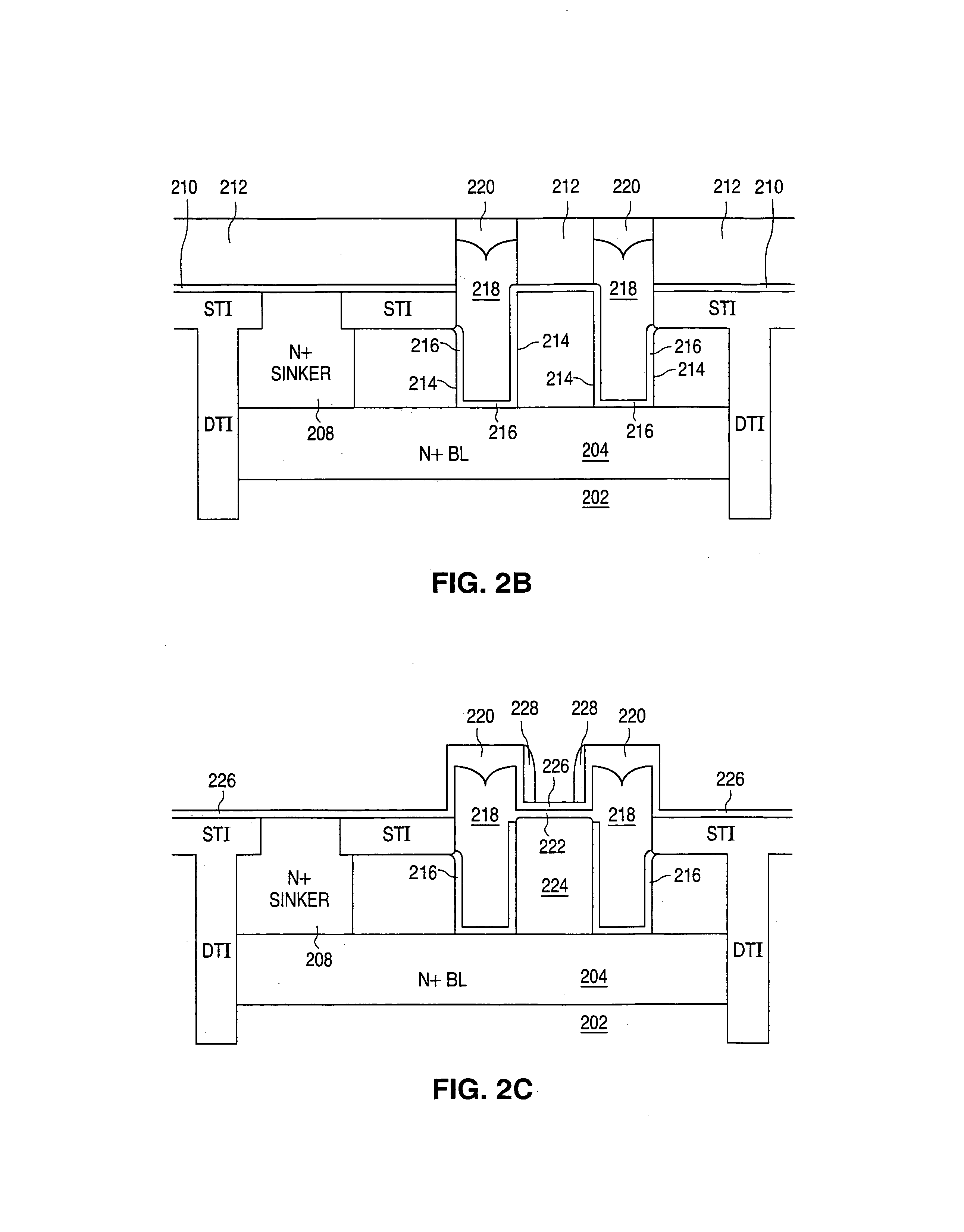
[0013]A super self-aligned bipolar junction transistor (BJT) structure, and a method of fabricating the structure, in accordance with the concepts of the invention, will now be described with reference to FIGS. 2A–2D. Specifics of the BJT structure and of the fabrication method, such as, for example device feature size, material layer thickness and dopant concentrations, are not provided, since, as will be appreciated by those skilled in the art, these parameters will vary depending upon the device application and are not germane to the concepts of the invention.

[0014]FIG. 2A shows a well-known “starting” structure for a bipolar junction transitor to be formed in a substrate 202 of crystalline silicon. The FIG. 2A structure includes an N+ buried layer (BL) 204 that serves as the BJT collector region formed on the upper surface of the silicon substrate 202. A layer 206 of collector epitaxial silicon is formed on the N+ buried layer 204; preferably, the doping level in the epitaxial l...


PUM


Abstract

A bipolar junction transistor (BJT) structure and fabrication method are provided in which a doped polysilicon filled trench is utilized to form both the extrinsic base contact region and a vertical field plate. A sacrificial mandrel of dielectric material is formed over regions that will become the BJT active area. This allows the polysilicon filled trench to be extended above the original semiconductor substrate surface. In this way, the base-collector and emitter-base junctions are both self-aligned to the field plate trench. The field plate is utilized to control and shape the electric field in the base-collector depletion region, allowing heavier collector well doping for the same breakdown voltage. This results in improvement in both the breakdown/Ron ratio and the fT*BVcbo product.

Description

TECHNICAL FIELD[0001]The present invention is directed to a bipolar junction transistor (BJT) structure, and to a method of fabricating the structure, in which the base-collector and emitter-base junctions are both self-aligned to a field plate trench etch, thereby providing a super self-aligned structure.BACKGROUND OF THE INVENTION[0002]As discussed by Raymond J. E. Hueting et al., “A New Trench Bipolar Transistor for RF Applications”, IEEE Transactions on Electron Devices, Vol. 51, No. 7, July 2004, it is well known that, for a high-voltage transistor, the tradeoff between the drift resistance and the breakdown voltage is improved by the reduced surface field (resurf) effect. The objective is to reshape the electric field distribution in the collector drift region for a reverse bias situation to form a more uniform field distribution with a reduced maximal field.[0003]Hueting at al. propose a vertical trench SiGe junction bipolar transistor (BJT) that improves the tradeoff between...

Claims


Application Information

Patent Timeline
IPC IPC(8): H01L21/331H01L21/8222
CPCH01L29/1004H01L29/407H01L29/42304H01L29/7378
Inventor KNORR, CHRISTOPHER J.
Owner NAT SEMICON CORP
Why Eureka
Try Eureka