Vertical field effect transistor on oxide semiconductor substrate

a technology of semiconductor substrates and transistors, which is applied in the direction of semiconductor devices, electrical equipment, basic electric elements, etc., can solve the problems of silicon-based vfets that cannot operate at high voltages, and silicon-based vfets that are not amenable to operating at high voltages

Inactive Publication Date: 2013-02-21
RAMGOSS
View PDF9 Cites 53 Cited by
  • Summary
  • Abstract
  • Description
  • Claims
  • Application Information

AI Technical Summary

Problems solved by technology

However, silicon-based VFETs have fundamental limitations.
First, silicon-based VFETs cannot operate at high voltages because of the silicon's properties.
Therefore, silicon-based VFETs are not amenable to operating at high voltages.
However, SiC-based VFETs are expensive to manufacture.
Because such a thick SiC epitaxial layer is required, the levelized cost to manufacture a SiC-based VFET can be up to 100 times more expensive compared to a silicon-based VFET.
Furthermore, the on-resistance of a SiC epitaxial layer can be high, which can limit the performance of the SiC-based VFET.
The high cost of manufacturing, as well as limited performance, slowed the adoption of SiC in power transistors.

Method used


Image

  • Vertical field effect transistor on oxide semiconductor substrate
  • Vertical field effect transistor on oxide semiconductor substrate
  • Vertical field effect transistor on oxide semiconductor substrate

Examples


Embodiment Construction

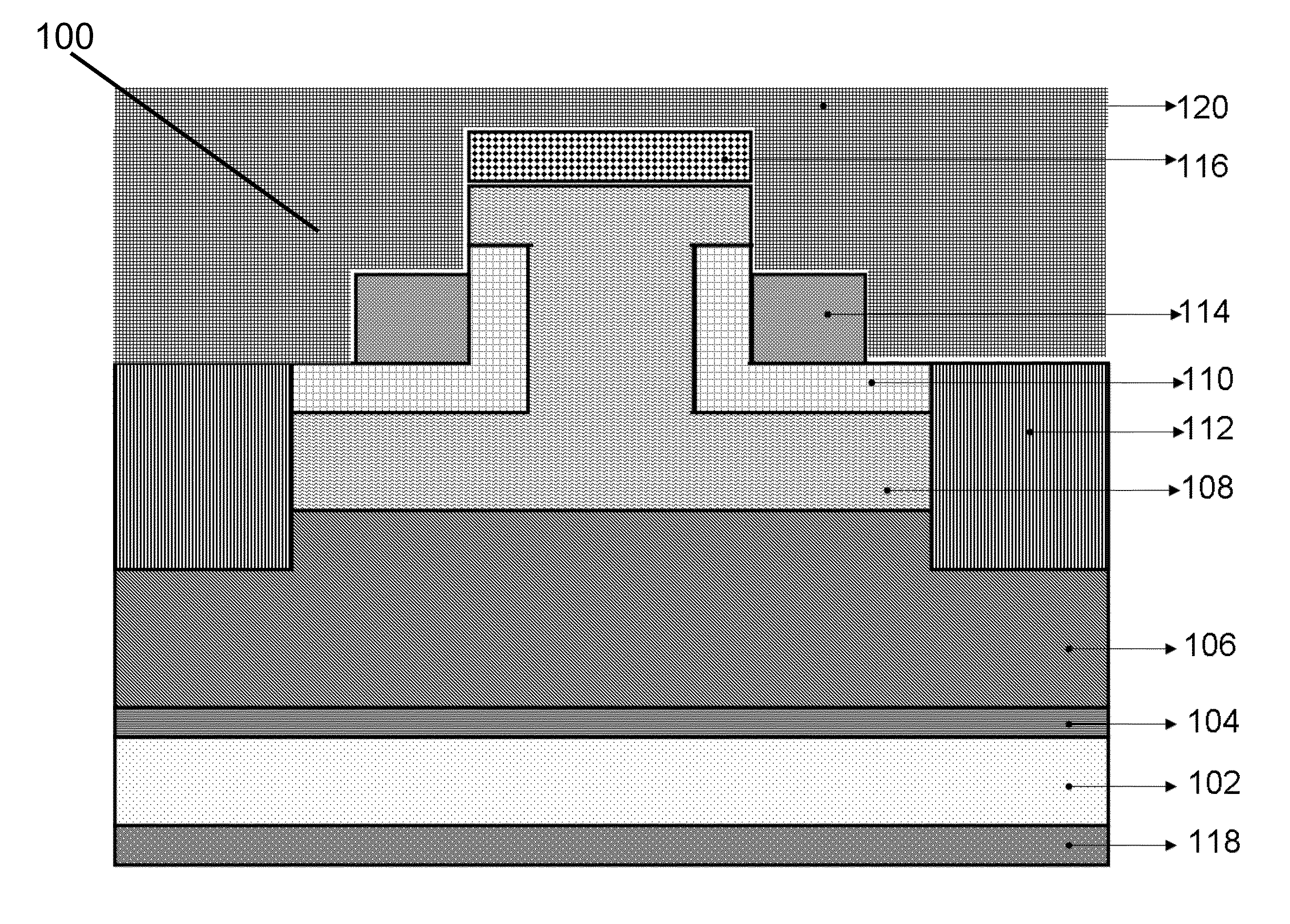
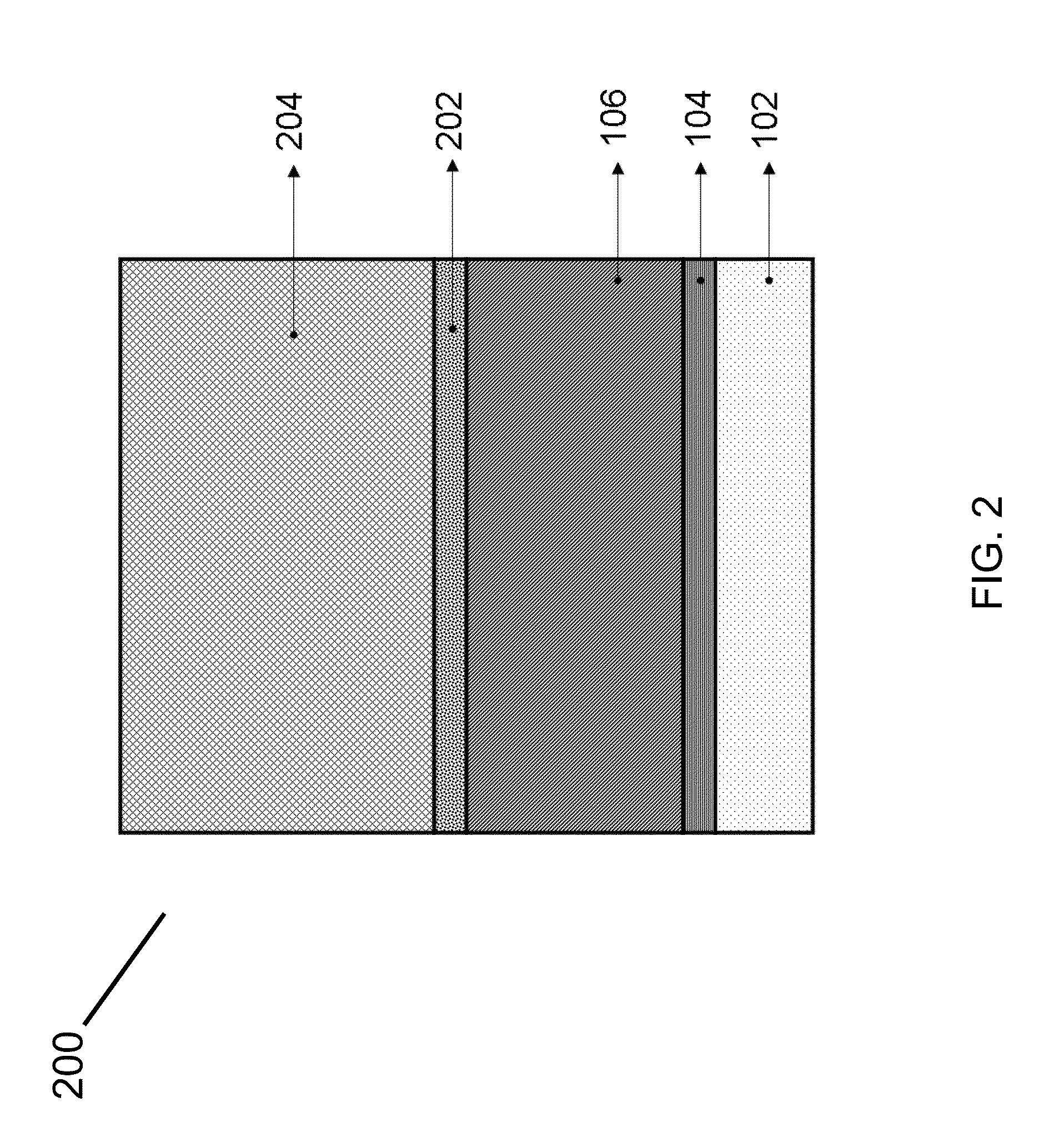
[0056]Reference now will be made in detail to embodiments of the disclosed subject matter. Such embodiments are provided by way of explanation of the disclosed subject matter, and the embodiments are not intended to be limiting. In fact, those of ordinary skill in the art can appreciate upon reading the specification and viewing the drawings that various modifications and variations can be made.

[0057]Before explaining at least one embodiment of the disclosed subject matter in detail, it is to be understood that the disclosed subject matter is not limited in its application to the details of construction and to arrangements of the components set forth in the following description or illustrated in the drawings. The disclosed subject matter can be manifested in other embodiments and of being practiced and carried out in various ways. Also, it is to be understood that the phraseology and terminology employed herein are for the purpose of description and should not be regarded as limiti...


PUM

PropertyMeasurementUnit
thicknessaaaaaaaaaa
widthaaaaaaaaaa
energy band gapaaaaaaaaaa

Abstract

A transistor, such as a vertical metal field effect transistor, can include a substrate including a ZnO-based material, and a structure disposed on a first side of the substrate comprising of AlGaN-based materials and electrodes disposed on the second side of the substrate. The transistor can also include a plurality of semiconductor layers and a dielectric layer disposed between the plurality of semiconductor layers and electrode materials.

Description

CROSS-REFERENCE TO RELATED APPLICATIONS[0001]This application claims the benefit under 35 U.S.C. §119(e) of the earlier priority date of U.S. Provisional Patent Application No. 61 / 524,510 entitled “Vertical Metal Insulator Semiconductor Field Effect Transistor,” by Bunmi Adekore, filed on Aug. 17, 2011, which is expressly hereby incorporated by reference herein in its entirety.BACKGROUND[0002]1. Technical Field[0003]The disclosed subject matter relates generally to metal insulator field effect transistors and methods of making the same, and more specifically to vertical field effect transistors and metal insulator field effect transistors comprising of group-III nitride materials and / or zinc insulator based semiconductor field effect transistors.[0004]2. Description of the Related Art[0005]A vertical field effect transistor (VFET) is a unique class of a three terminal transistor. A VFET includes source, drain and gate electrode terminals, and the VFET sustains electric fields betwee...

Claims


Application Information

Patent Timeline
Patent Type & Authority Applications(United States)
IPC IPC(8): H01L29/78H01L21/336
CPCH01L29/267H01L29/22H01L29/66454H01L29/66462H01L29/66522H01L29/66924H01L29/66969H01L29/7788H01L29/7789H01L29/7802H01L29/7813H01L29/8083H01L29/045H01L29/0615H01L29/0657H01L29/0847H01L29/1066H01L29/2003H01L29/66446
Inventor ADEKORE, BUNMI T.
Owner RAMGOSS
Why Eureka
Try Eureka