Optoelectronic device having surface periodic grating structure

a technology of periodic grating and optoelectronic devices, which is applied in the direction of sustainable manufacturing/processing, climate sustainability, semiconductor devices, etc., can solve the problems of increasing the complexity and time consumption of the manufacturing process, and achieves simplified and fast manufacturing processes, enhanced optoelectricity of the optoelectronic device, and increased the resonance of the incident light and the active region

Inactive Publication Date: 2016-09-20
KINGWAVE
View PDF7 Cites 2 Cited by
  • Summary
  • Abstract
  • Description
  • Claims
  • Application Information

AI Technical Summary

Benefits of technology

[0003]An objective of the present invention is to provide an optoelectronic device having a surface periodic grating structure, such that a direction of the incident light is changed to become a horizontal light parallel to the surface of the multi-layer semiconductor structure layer and resonant to the multi-layer semiconductor structure layer, such that a transmitting path of the incident light in the multi-layer semiconductor structure layer is extended to enhance optoelectricity of the optoelectronic device.
[0004]Another objective of the present invention is to provide a method of forming an optoelectronic device having a surface periodic grating structure, which does not require additional steps to form the metal grating thin film and dielectric layers, and may enhance the optoelectricity of the optoelectronic device by etching the multi-layer semiconductor structure layer to form a periodic grating structure layer embedded therein.
[0005]To achieve the aforementioned and other objectives, an aspect of the present invention provides an optoelectronic device having a surface periodic grating structure, which includes: a substrate; a multi-layer semiconductor structure layer formed on the substrate; and a periodic grating structure layer embedded in the multi-layer semiconductor structure layer by etching, the periodic grating structure layer being performed with a design on a surface of the multi-layer semiconductor structure layer based on parameters including an optimized period, a filling factor and a depth. The substrate, the multi-layer semiconductor structure layer and the periodic grating structure layer form the optoelectronic device. An incident light to the optoelectronic device is configured to pass through the periodic grating structure layer to enter the multi-layer semiconductor structure layer, and a direction of the incident light is changed to become a horizontal light parallel to the surface of the multi-layer semiconductor structure layer and resonant to the multi-layer semiconductor structure layer, such that a transmitting path of the incident light in the multi-layer semiconductor structure layer is extended to enhance optoelectricity of the optoelectronic device. In certain embodiments, the multi-layer semiconductor structure layer includes at least one of an infrared detector structure, a visible light detector structure, an ultraviolet light detector structure, or a solar cell structure, and a waveband frequency spectrum of the incident light is between visible light and far infrared spectrum (300 nm˜24 um).
[0007]Comparing to the known arts, the optoelectronic device and the manufacturing method thereof includes the following advantages and characteristics: 1. The present invention does not require additional steps to form the metal grating thin film and dielectric layers, and may enhance the optoelectricity of the optoelectronic device by etching the multi-layer semiconductor structure layer to form a periodic grating structure layer embedded therein, which is different from the conventional surface plasma resonant technology, and has a simplified and fast manufacturing process. 2. The periodic grating structure of the present invention is formed in the active region or deeper region, which extends the transmitting path of the incident light in the multi-layer semiconductor structure layer, and increases the resonance of the incident light and the active region, such that the optoelectricity of the optoelectronic device is enhanced. 3. The period of the periodic grating structure of the present invention may be determined to be an optimized dimension based on the incident light with different wavelength, such that the light satisfies the resonance condition, and may be transmitted horizontally in the active region of the optoelectronic device to enhance the optoelectricity of the optoelectronic device.

Problems solved by technology

However, surface plasma resonance techniques must be performed with the existence of both the metal layer and non-conductive dielectric layer, and a metal grating thin layer and a dielectric layer are required, which increases the complexity and time consumption of the manufacturing process.

Method used


Image

  • Optoelectronic device having surface periodic grating structure
  • Optoelectronic device having surface periodic grating structure
  • Optoelectronic device having surface periodic grating structure

Examples


Embodiment Construction

[0023]To understand the objectives, features and effects of the present invention, the following detailed description of the embodiment of the present invention is provided along with the accompanied drawings to further describe the present invention in greater detail as follows.

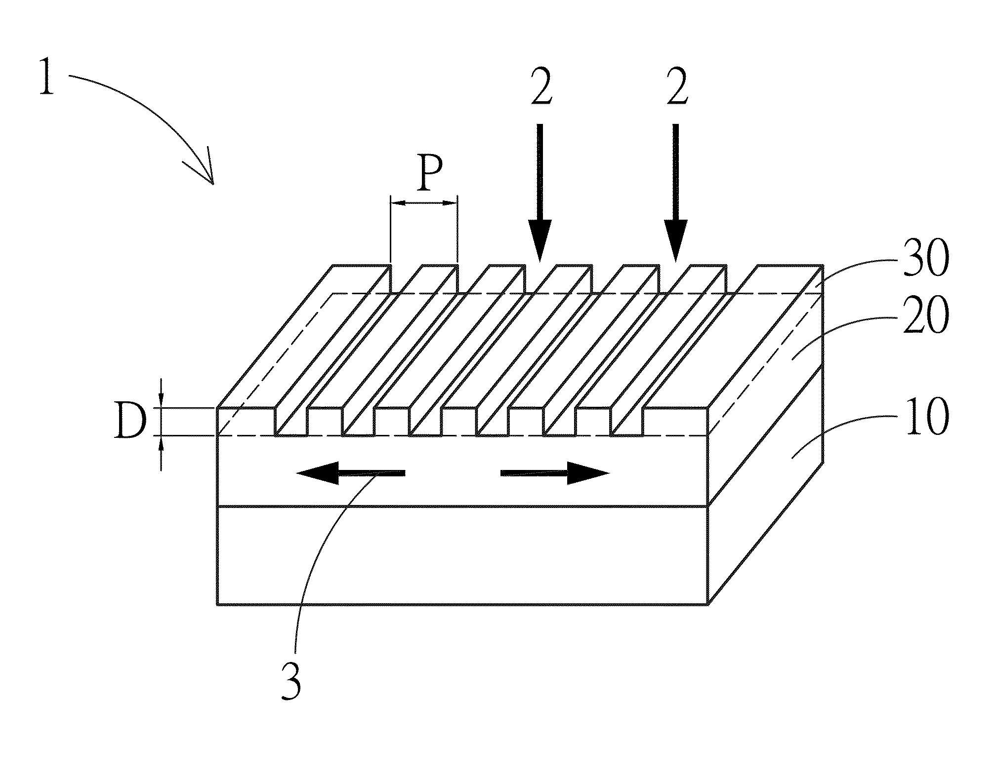
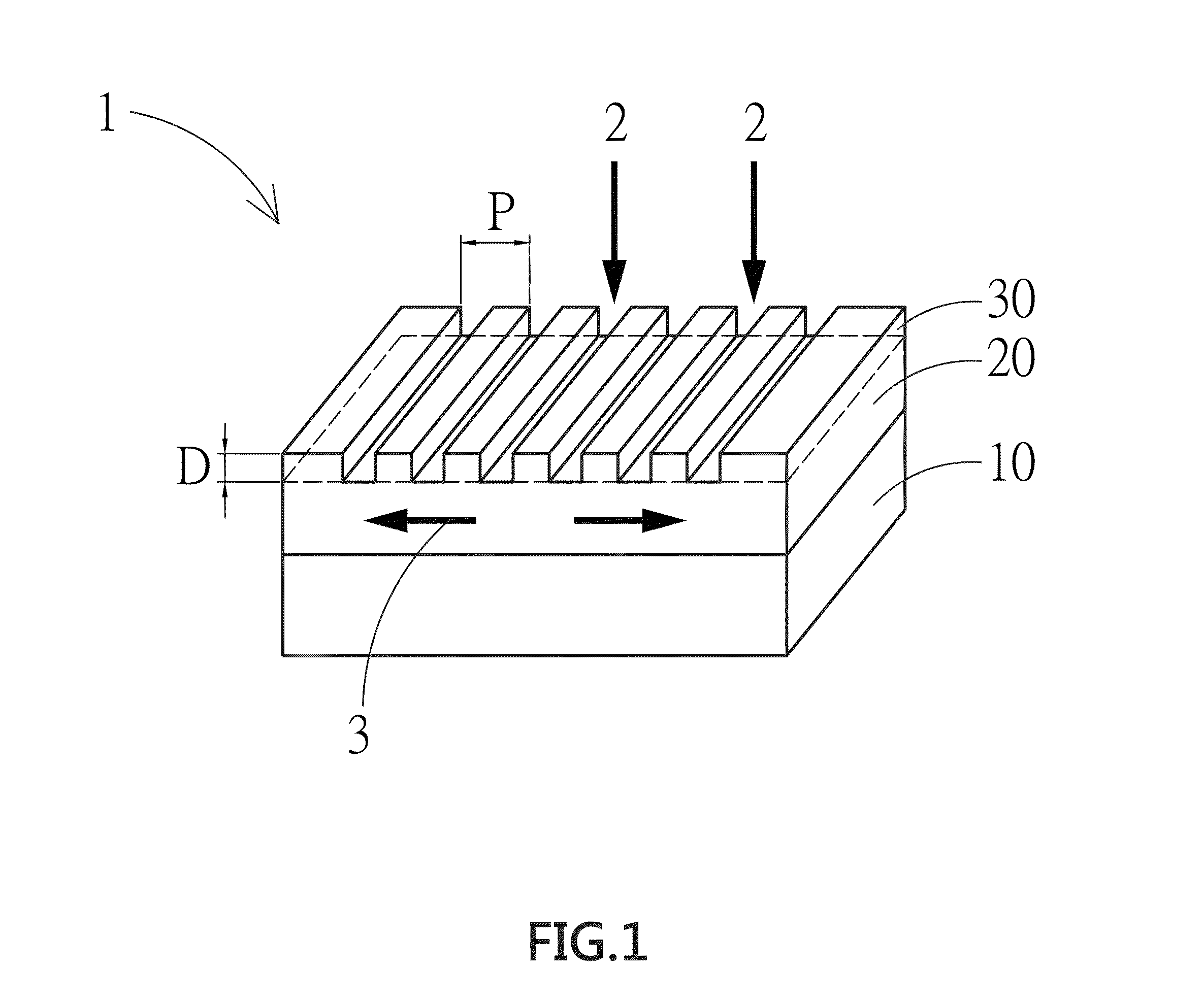
[0024]Refer now to FIG. 1, which shows a schematic view of an optoelectronic device having a surface periodic grating structure according to an embodiment of the present invention. The optoelectronic device has a substrate 10, a multi-layer semiconductor structure layer 20 and a periodic grating structure layer 30. The substrate 10, the multi-layer semiconductor structure layer 20 and the periodic grating structure layer 30 form the optoelectronic apparatus 1. An incident light 2 to the optoelectronic apparatus 1 is configured to pass through the periodic grating structure layer 30 to perform diffraction and transmittance, and to enter the multi-layer semiconductor structure layer 20. When the wavelength of ...


PUM


Abstract

The present invention provides a optoelectronic device having a surface periodic grating structure and a manufacturing method thereof, which includes: a substrate; a multi-layer semiconductor structure layer formed on the substrate; and a periodic grating structure layer embedded in the multi-layer semiconductor structure layer by etching based on optimized parameters. A direction of an incident light to the optoelectronic device is changed to be resonant to the multi-layer semiconductor structure layer to enhance optoelectricity of the optoelectronic device. The method includes: (1) providing a substrate; (2) forming a multi-layer semiconductor structure layer on the substrate; (3) selecting parameters to perform a design for a periodic grating structure layer on a surface of the multi-layer semiconductor structure layer; and (4) forming the periodic grating structure layer embedded in the multi-layer semiconductor structure layer by etching.

Description

FIELD OF THE INVENTION[0001]The present invention relates to an optoelectronic device and the manufacturing method thereof, and particularly to an optoelectronic device having a surface periodic grating structure and the manufacturing method thereof.BACKGROUND OF THE INVENTION[0002]With the rapid technology development nowadays, optoelectronic elements have become widely used in our daily lives. In recent years, research to the optoelectronic elements has focused on enhancing the efficiency of the optoelectronic elements. Typically, optoelectronic elements may include photodetectors and solar cells. Implementations of the photodetectors include visible light detectors, which are photodetectors that can be utilized in the digital cameras, and optical pickup heads of digital optical drives. Generally, the surface of a visible light detector may be applied with surface plasma effect to strengthen the incident light such that efficiency may be enhanced. For example, Taiwan Patent No. 13...

Claims


Application Information

Patent Timeline
Patent Type & Authority Patents(United States)
IPC IPC(8): H01L31/0232H01L31/105H01L31/0352H01L31/18
CPCH01L31/02327H01L31/035236H01L31/105H01L31/1844Y02E10/52Y02E10/544Y02P70/50
Inventor KUAN, CHIEH-HSIUNGLEE, MING-LUN
Owner KINGWAVE
Why Eureka
Try Eureka